
| Generations |
Pre-3D (-1995) Texture Mappers (1995-1999) Fixed T&L, Early Shaders (2000-2002) Shader Model 2.0/3.0 (2003-2007) Unified Shaders (DX10-11) Featureset determines where a card will go, not its year of introduction |
||||||||||||||||||||||||||||||||||||||||||||||||||||||||||||||||||||||||||||||||||||||||||||||||||||||
| Unified Shader? GPGPU? |
Around 2004 time, when SM3.0 was new and cool, we were noticing from framerate profiling that some frames, roughly one or two a second, took far more rendering time than all others. This caused "micro-stutter", an uneven framerate. The shader profile showed that these frames were much more vertex shader intensive than the others and GPUs had much less vertex shader hardware than pixel shader hardware, because most frames needed about a four to one mix. As shader units were getting more and more complex, it made sense for each shader to be able to handle both vertex and pixel programs. ATI introduced this with the Radeon HD2xxx series, though due to other "features" on the GPU, they were generally slower than the previous generation X1xxx series. Nvidia jumped on board with the Geforce 8 series, with 500 MADD GFLOPS on the top end Geforce 8800 parts. The teraflop GPU was in sight. The first GPU with enough shaders running fast enough to be able to manage one trillion operations per second was the AMD Radeon HD4850, though the previous generation 3870 X2 had surpassed this, it was two GPUs on one card. Nvidia struggled during this generation, while the Geforce GTX285 did manage to hit one TFLOPS, it was expensive, noisy, power hungry and rare. | ||||||||||||||||||||||||||||||||||||||||||||||||||||||||||||||||||||||||||||||||||||||||||||||||||||||
| MADD? FMA? |
The most complex operation an FPU historically did was the "multiply-add" (MADD) or "fused-multiply-add" (FMA). It's doing a multiply and an add at the same time. The operation is effectively an accumulate on value a where a = a + (b x c) and the distinction is that intermediate value b x c in a MADD is rounded to final precision before it is added to a, while in an FMA, the intermediate is at a higher precision and not rounded before the add, only the final value is rounded. The real-world distinction is minor and usually ignorable but for FMA being performed in a single step, so typically twice as fast. AMD introduced FMA support in TeraScale 2 (Evergreen, 2009) and Nvidia in Fermi (2010). A common driver optimisation is to promote MADD operations to FMA. For consistency's sake, where we list "MADD GFLOPS" or "FMA GFLOPS", we may mean either, whichever one is fastest on the given hardware. An FMA, despite being treated as one operation, is actually two and therefore if a GPU can do one billion FMAs a second, its GFLOPS (giga-floating point operations per second, 1 GFLOPS is one billion ops per second) is 2. However, FMA performance does carry the implication of it being "two in one", so a GPU's throughput in other operations is half that. FMA is important, dot products and matrix multiplication intensively use FMA, as do convolutions, as in a convolutional neural network. FMA also allows more efficient calculations of square roots and divisions. So, if we work out the throughput of a GPU in purely number of operations it can do in any given second (let's have a hypothetical RTX 2070 running at 2.0 GHz)... CUDA cores = 2304 Clock = 2.0 (as this is in GHz, our result will be in billions of operations per second, GFLOPS) Nice and simply, we just multiply the number of cores by the clock. This assumes all cores do useful work in every clock tick for one second. This almost never really happens. 2304 x 2.0 = 4,608 GFLOPS If you just run a lot of parallel very tight loops of FP32 adds or multiplies in CUDA code, this is the number you'll measure. If you start running real code, where the compiler can throw FMA into the mix (and it will, this is a very low hanging fruit for compiler optimisation), you'll find your results climb above the theoretical maximum we calculated just now. If, however, your measurements are clever and count an FMA as one operation, they will not. | ||||||||||||||||||||||||||||||||||||||||||||||||||||||||||||||||||||||||||||||||||||||||||||||||||||||

|
PNY GeForce 8800 GTS 512 MB - 2007 It's fitting that we lead this article with the GeForce 8800, which was the first DirectX 10 class GPU, the first use of unified shaders, the first implementation of Nvidia's new "Tesla" architecture, which was still called G80 back then. What we understand a modern GPU to be, this was the first. As a popular card, there were a lot of variants, and PNY's lot usually used its "XLR8" branding, but this one used Nvidia's reference branding. What G80 did was make very simple ALUs which could be double-pumped. The G80 architecture did SIMD over eight "stream processors" (later to be called CUDA cores) which were natively FP32. With 16 "streaming multiprocessors" (SMs), G80 had 128 stream processors. It clocked them to 1,200 "MHz-equivalent" in most G80s, but the rest of the GPU clocked at a more sensible 600 MHz. This double pumped ALU stack was using clock doubling, so it triggered on the rising and falling edges of the clock. The shader domain on G80/Tesla/Fermi ran the ALUs at the double-pumped "shader domain" clock, but the supporting structures, such as cache, registry, flow control, special functions, dispatch and retire only ran at the base clock. The original 8800 GTS had a 320 MB variant with 12 SMs and a 640 MB variant with 14 SMs. They used the G80 GPU on TSMC's 90 nm process. When 65 nm came along, Nvidia was soon transitioning over to it, and the G92 GPU was the result. It had the same 16x8 streaming processor configuration, but was a lot smaller, 324 mm^2 instead of G80's 480. This GTS 8800 512MB was a G92 and was configured almost identically to the GeForce 9800 GTX. In the 8800 GTS 512 MB, G92 was clocked higher than its G80 predecessor, with a shader domain of 1625 MHz and a GPU clock of 812.5 MHz. G92 was not a direct die shrink of G80, it was a little more capable in its CUDA configuration (Compute Capability 1.1, not 1.0), but the 55 nm G92b was a direct die shrink of G92. G92 improved the PureVideo IP block, meaning VC-1 and H.264 could be GPU assisted. G92 also had an alarming incompatibility with PCIe 1.0a motherboards, which led to the video card not initialising during boot. This caused a very high return rate, as Nvidia's backwards compatibility (something the PCIe specification demands) only went as far back as PCIe 1.1. Nvidia's spec for the memory was 820 MHz GDDR3, but most vendors used faster RAM. The 8800 and 9800 series were just before Nvidia started to lose the plot a little. Tesla's extreme shader clocks served it well for small pixel shader programs of the sort DX9 would use. G80 was up against ATI's RV670, which had 320 cores, but in a VLIW-5 design. While VLIW-5 was harder to get peak performance from, it used fewer transistors, less die area and so resulted in a smaller, cheaper GPU - It also used much less power. A product line as popular as the 8800 series was means it was influential. Games even as far as 2015, eight years later, would often say a 8800 GT or GTS was the minimum requirement. While ATI's RV670 in, say, Radeon HD 3870 (8800 GTS's most direct competitor) had a board power of just over 100 watts, 8800 GTS was rated at 150 watts. So far, so good. By the time reach 2009, two years later, we have Radeon HD 5870's Cypress GPU against Tesla's swansong, GT200B, we have ATI's 180 watt board power against Nvidia's 238 watt GeForce GTX 285. Ultimately it was not possible for Nvidia to keep throwing more and more power at the problem. Nvidia PureVideo (VDPAU), the SIP block doing video decode tasks, was second generation, which could handle H.264 up to 2K resolution, but had only partial VC-1 support. MPEG-2 and MPEG-4 SP/ASP were fully handled. Core: 16 ROPs, 32 TMUs, 650MHz (20.8 billion texels per second, 10.4 billion pixels per second) RAM: 256 bit GDDR3, 970MHz, 62,080MB/s Shader: 16x Unified shader 5.0 (16 SIMD of 8, 128 total) MADD GFLOPS: 416 Most recent driver is 342.01 from 2016, when G80/G9x class Tesla support was dropped. | ||||||||||||||||||||||||||||||||||||||||||||||||||||||||||||||||||||||||||||||||||||||||||||||||||||||
|
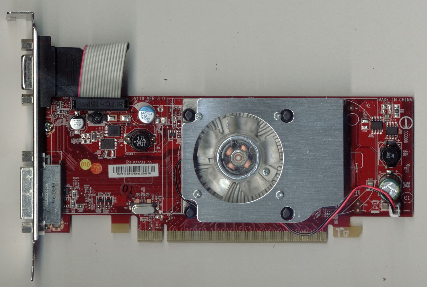
MSI Radeon HD3450 (V118 R3450-TD256H Hewlett Packard OEM variant) - 2007 All I had for this was an Underwriters Laboratories certification number, E96016 which identified it as nothing beyond the basic PCB manufactured by Topsearch of Hong Kong and the model number, V118. That's not a lot to be going on. It came out of a HP Pavillion desktop, pretty typical consumer junk and certainly nothing intended for gaming, so it's not going to be anything spectacular (the size of the PCB says that too). All hardware tells a story, it's just a matter of listening. The silkscreening on the PCB tells us that it's got guidelines for quite a few different coolers, this PCB is meant for a family of video cards perhaps all based around the same GPU or similar GPUs. The VGA connector can be omitted easily and isn't part of the PCB - It's aimed at OEMs who know what they want and need no flexibility. It's a Radeon HD3450 with 256MB manufactured by MSI using a Topsearch manufactured PCB. It's amazing what the right search terms in Google can let you infer, isn't it? MSI's standard retail part comes with a large passive heatsink and S-video out, but OEMs can get whatever variant of a design they like if it'll seal a deal for thousands of units. These things, the V118 model, were retailing at about $20. Under the heatsink is a 600MHz RV620 (A near-direct die shrink to 55nm of the HD2400's 65nm RV610) GPU feeding 1000MHz GDDR2 memory, but the good ends there. The memory is 64 bit, giving a meagre 8GB/s bandwidth and the core has only four ROPs - It's a single quad. Unified shader 4.1 is present, 40 units, but they're pretty slow. Core: RV620 with 4 ROPs, 1 TMU per ROP, 600MHz (2.4 billion texels per second, 2.4 billion pixels per second) RAM: 64 bit DDR2, 1000MHz, 8000MB/s Shader: 1x Unified shader 4.1 MADD GFLOPS: 48 |
||||||||||||||||||||||||||||||||||||||||||||||||||||||||||||||||||||||||||||||||||||||||||||||||||||||
|
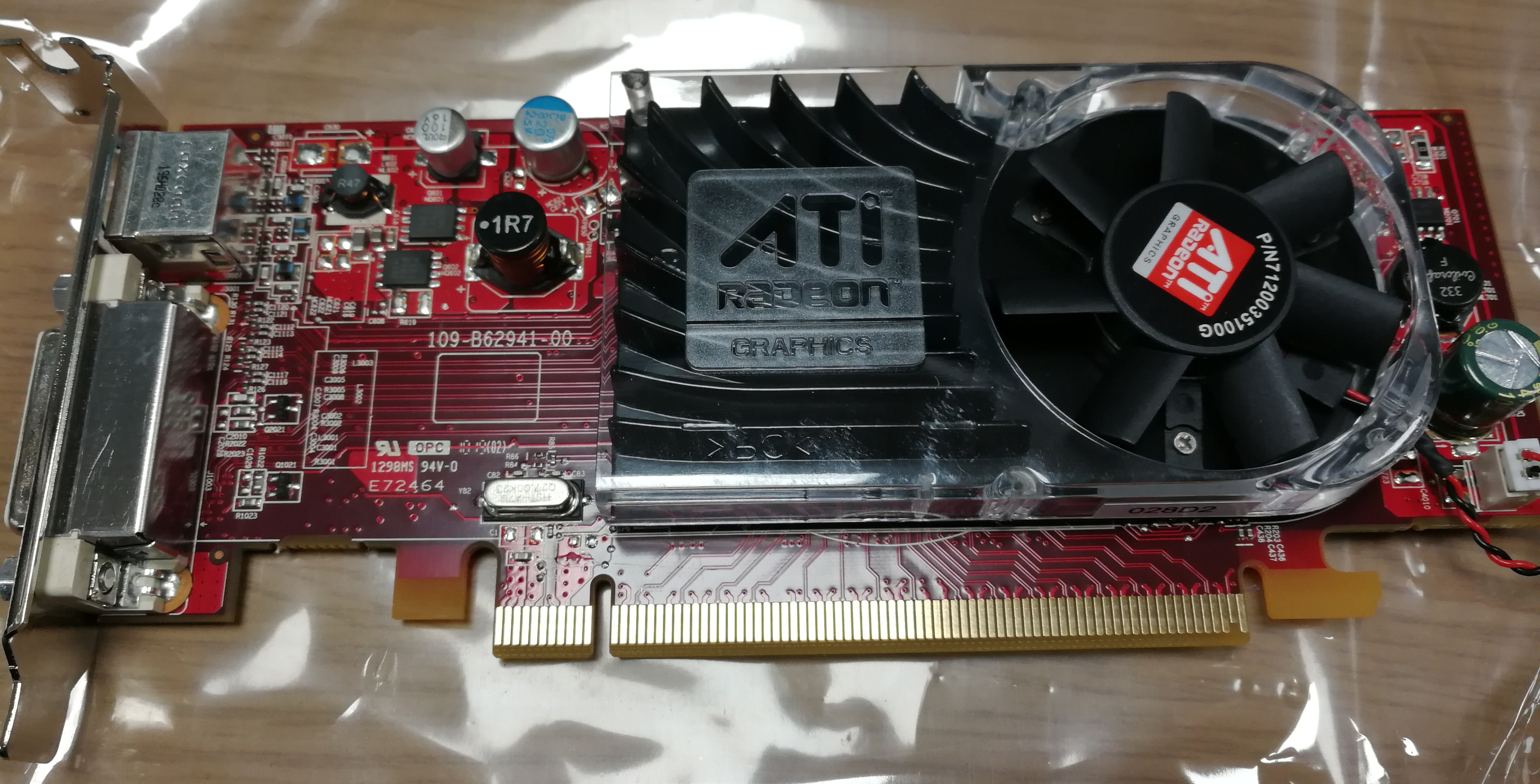
ATI Radeon HD 3450 256 MB (AMD B629 Dell OEM variant as 'W337G') - 2007 ATI's OEM parts were never easy to identify. This one carried its FCC identification as ADVANCED MICRO DEVICES MODEL: B629, dating it to after AMD's acquisition of ATI. The PCB carries a date code showing it was made in week 19, 2010. The rear connector carries a DMS-59 output and the standard-for-the-time S-Video output. Looking at the size and layout of the PCB shows us that it is clearly a derivative of the one above with many components sharing identical placement. Notably, this one has a half-height bracket for the Dell Optiplex SFF 360/380/755/760/780. The performance of the Radeon HD 3450's RV620 GPU was, to a word, lacking. It carried DDR2 memory as standard, running it at 500 MHz for just 8 GB/s memory bandwidth. The memory was provided by SK Hynix as four BGA packages, two on each side. At 600 MHz the GPU itself was never going to set any records, especially with just one R600-architecture shader package (40 individual shaders). Getting more performance out of this was an exercise in how highly the RAM would clock. Even with the down-clocked GPU, 8 GB/s plain was not enough. The GPU itself would normally hit 700-800 MHz (and in the HD 3470, the same GPU was running at 800 MHz on the same PCB, with the same cooler!) but this didn't help when the RAM was slow 64 bit DDR2. When it arrived here, in 2019, it had been sat in a corporate stock room for years and was completely unused, not a single grain of dust on the fan. On power on, as was common for GPUs of the day, the fan spins up to maximum before winding back. This is really quite noisy for such a small fan! No amount of persuasion or different systems got anything recognising it as a video card, or even that a video card was present. We'll talk about the GPU architecture on this one, since the actual card was not functional. R600 used a ring bus to connect the ROPs to the shader cores, a rather unusual architecture, and took a VLIW-5 instruction set later back-named TeraScale 1. This means each shader block of 40 was eight individual cores, which could handle a single VLIW-5 instruction to its five execution units. TeraScale 2 would increase this to sixteen cores (and 80 shaders per block). R600's ring bus also, as noted, decoupled the ROPs from the execution units, but the texture units were "off to one side" of the ring bus, so each group of execution units did not have its own samplers and combining samples with pixels to do MSAA meant first colour data exiting the shaders into the ring bus, then into the texture units, then back to the ring bus to head to the ROPs to be finally MSAA sampled. This was inefficient and, in the original R600, plain didn't work. Even in the revised silicon, which RV620 here is based on, it was best to avoid antialiasing. The RV620 also improved the UVD video block from "1.0" to "2.0", adding better video decoding to the GPU. Physically, the GPU was 67 mm^2 and contained 181 million features. At 67 mm^2, it barely cost anything to make. It would be AMD's smallest GPU until Cedar/RV810, three years later in 2010, at 59 mm^2. A drop in the price of bulk silicon from TSMC after 28 nm and the general increase in very low end GPU cost meant that no subsequent GPU has been this small, though Nvidia's 77 mm^2 GP108 came close. Powerful IGPs from AMD and Intel embedded in the CPUs have put paid to the very small die entry level GPU segment. Core: RV620 with 4 ROPs, 1 TMU per ROP, 600MHz (2.4 billion texels per second, 2.4 billion pixels per second) RAM: 64 bit DDR2, 1000MHz, 8000MB/s Shader: 1x Unified shader 4.1 MADD GFLOPS: 48 | ||||||||||||||||||||||||||||||||||||||||||||||||||||||||||||||||||||||||||||||||||||||||||||||||||||||
|
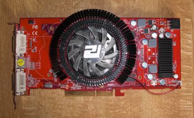
PowerColor Radeon HD 3850 AGP 512MB - 2007 If one were to chart all the GPUs made since the early DX7 era, he would notice a near-perfect rule applying to the industry. One architecture is used for two product lines. For example, the NV40 architecture was introduced with Geforce 6 and then refined and extended for Geforce 7. There's an entire list covering the whole history of the industry. Observe:
What's happening is that a new GPU architecture is made on an existing silicon process, one well characterised and understood. ATI's R600 was on the known 80nm half-node process, but TSMC quickly made 65 nm and 55 nm processes available. The lower end of ATI's Radeon HD 2000 series were all 65 nm, then the 3000 series was 55 nm. The die shrink gives better clocking, lower cost and better performance, even if all else is equal. It's also an opportunity for bugfixing and fitting in those last few features which weren't quite ready first time around. In ATI's case, the Radeon HD 2 and 3 series are the same GPUs. Here's a chart of what uses what:
Whew! ATI used the R600 architecture across three product lines, making it almost as venerable as the R300, which was used across three lines and in numerous mobile and IGPs. ATI used R300 so much because it was powerful and a very good baseline. So what of R600? To a word, it sucked. The top end 2900 XTX was beaten by the previous generation X1900 XT, let alone the X1950s and the top of the line X1950 XTX. It suffered a catastrophic performance penalty from enabling antialiasing and Geforce 7 could beat it pretty much across the board: Yet here was a product meant to be taking on Geforce 8! While this was released in 2008 (announced in January, but was in the channel by December the previous year), the PCIe version was 2007, so that is listed as the year here. ATI did, however, throw the price really low. You could pick them up for £110 when new and even as I wrote this entry (August 2009) they were still in stock for around £75. There'd not been a really decent mid-range card since the Geforce 6600GT (though the Geforce 7900GT was fairly mid-range, it was overpriced) and the ageing Geforce 7 series was still available, it was not at the DirectX 10 level. The ATI Radeon HD 3850 pretty much owned the mid-range of the market. Better still, it was available in this AGP version which wasn't a cut down or in any way crippled model as most AGP versions were. Indeed, Sapphire's AGP version was overclocked a little and both Sapphire and PowerColor's AGP cards had 512 MB of memory, up from the standard 256 MB. The PowerColor card used this very large heatsink but Sapphire used a slimline single-slot cooler. In early 2008, these were a damned good buy, especially for the ageing Athlon64 X2 (or Opteron) or older Pentium4 system which was still on AGP. It's also a worth a mention about the Unified Video Decoder here. ATI called it the "Xilleon video processor" (because everything ATI branded was "-eon"), which was based on a licensed Tensilica Xtensa LX. It didn't offer MPEG-2 at this stage (MPEG-2 was easily a CPU task by this time) or MPEG-4 SP/ASP, but instead the more complex H.264 and VC-1 decoding up to the requirement of BluRay and HD-DVD. This basic capability would be retained with minor enhancement up to and including the Radeon HD 5000 generation. Core: RV670 with 16 ROPs, 1 TMU per ROP, 670MHz (10.7 billion texels per second, 10.7 billion pixels per second) RAM: 256 bit GDDR3, 1660MHz, 53,100 MB/s Shader: 4x Unified shader 4.1 MADD GFLOPS: 429 Supplied by Doomlord |
||||||||||||||||||||||||||||||||||||||||||||||||||||||||||||||||||||||||||||||||||||||||||||||||||||||
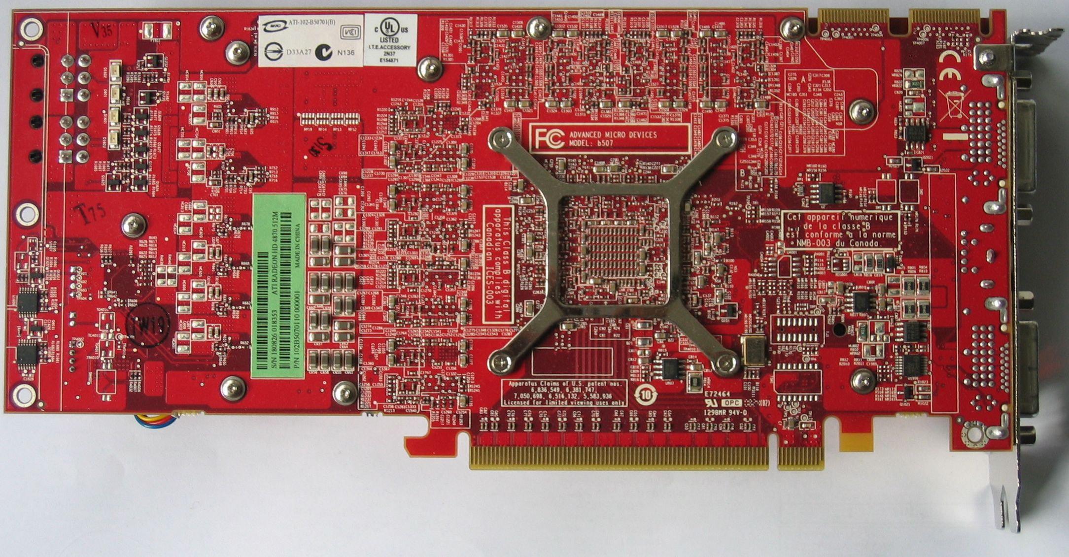 |
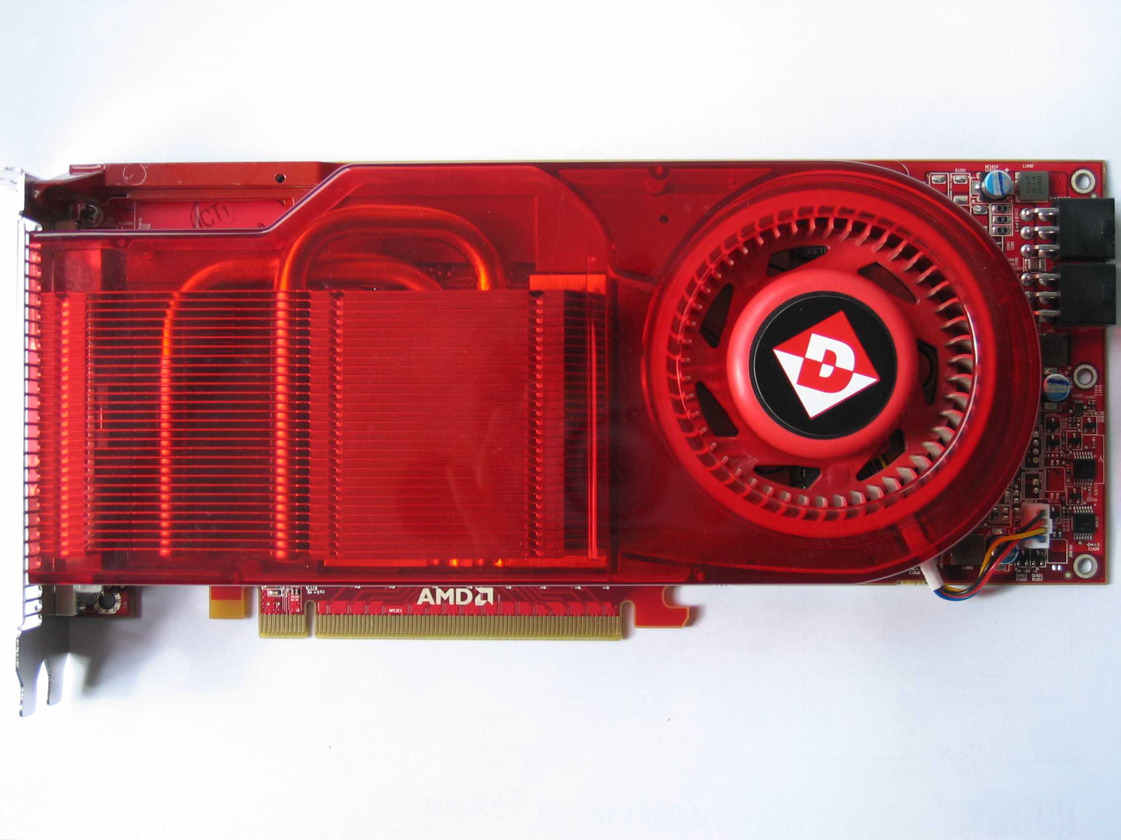
AMD Radeon HD 4870 - 2008 After losing their way somewhat with the Radeon HD 2xxx (R600) debacle, AMD were determined to set matters straight with the 3xxx and 4xxx series. The 3xxx were little more than bugfixed and refined 2xxx parts, comprising of RV620, 635 and 670 (though the RV630 was actually the Radeon HD 2600). ATI had postponed the R400/Loki project when it turned out to be far too ambitious and had simply bolted together two R360s to produce their R420, which powered the Radeon X800XT and most of the rest of that generation, sharing great commonality with the Radeon 9700 in which R300 had debuted. Indeed, a single quad of R300, evolved a little over the years, powers AMD's RS690 chipset onboard graphics as a version of RV370. By 2006, the R400 project still wasn't ready for release (ATI had been sidetracked in building chipsets, being bought by AMD) and R500, which R400's Loki project was now being labelled as, was still not ready. Instead, R520 was produced. It was quite innovative and the RV570, as the X1950, became one of the fastest things ever to go in an AGP slot. It also provided the XBox 360's graphics. It took until 2008 for what was the R400 to finally hit the streets as R600. All the hacks, tweaks and changes made to the chipset meant that it was barely working at all. Things as basic as antialiasing (which should have been handled by the ROPs) had to be done in shaders because the ROPs were rumouredly broken. This crippled the R600's shader throughput when antialiasing was in use and led to pathetically low benchmark scores. R700 corrected everything. Sporting unified shaders at 4.1 level (beyond DirectX 10) and eight hundred of them at that (these are raw ALUs, the RV770 contains ten shader pipelines, each with 16 cores, each core being 5 ALUs - It's more correct to say that RV770 contains 10 shaders, and 160 shader elements, what AMD call 'stream processors'), corrected the ring memory controller's latency issues and fixed the ROPs. After two generations of being uncompetitive, AMD were back in the ring with the RV710 (4450, 4470), RV730 (4650, 4670) and RV770 (4850, 4870). RV770's ROPs are again arranged in quads, each quad being a 4 pipeline design and having a 64 bit bus to the memory crossbar. Each pipeline has the equivalent of 2.5 texture mappers (can apply five textures in two passes, but only two in one pass) Worth comparing is a Radeon HD 2900XT: 742MHz core, 16 ROPs, 105.6GB/s of raw bandwidth, 320 shaders, but about a third of the performance of the 4870 - Even when shaders aren't being extensively utilized. Core: 16 ROPs, 40 TMUs, 750MHz (30.0 billion texels per second, 12.0 billion pixels per second) RAM: 256 bit GDDR4, 1800MHz, 115200MB/s (GDDR5 is dual ported, so is actually a form of QDR) Shader: 10x Unified shader 4.1 (80 units each) MADD GFLOPS: 1,260 It is apparently quite difficult to coax full performance out of the shaders, most synthetic benchmarks measure between 200 and 800 GFLOPS Thanks to Filoni for providing the part |
||||||||||||||||||||||||||||||||||||||||||||||||||||||||||||||||||||||||||||||||||||||||||||||||||||||

|
Nvidia Quadro FX 380 256 MB - 2008 The Quadro FX 380 used Nvidia's G96 GPU, and ran it at 450 MHz. It had 256 MB of GDDR3 RAM, running at 700 MHz. It used the Tesla architecure, had 16 shaders, 8 TMUs and 8 ROPs. It was rated for a very low 34 watt TDP. This meant it compared against the embarrasingly slow GeForce 9400 GT:
The significantly more powerful 9400 GT was also about a quarter of the price. The G96 GPU had four execution cores, each with 8 CUDA cores, but the Quadro FX 380 had half the entire GPU disabled. It, to a word, stank. Did you get ECC memory? No. Was it a top quality PCB? No, it was just a regular PNY manufactured PCB. Some components were rotated, like the VRM inductor and the RAM chips, but this is hardly unique to a Quadro, and PNY used almost the exact same PCB design on its 9500 GT Core: 4 ROPs, 8 TMUs, 450MHz (3.6 billion texels per second, 1.8 billion pixels per second) RAM: 128 bit DDR3, 700MHz, 22,400MB/s Shader: 2x Unified shader 4.0 (16 units) MADD GFLOPS: 28.8 | ||||||||||||||||||||||||||||||||||||||||||||||||||||||||||||||||||||||||||||||||||||||||||||||||||||||
|
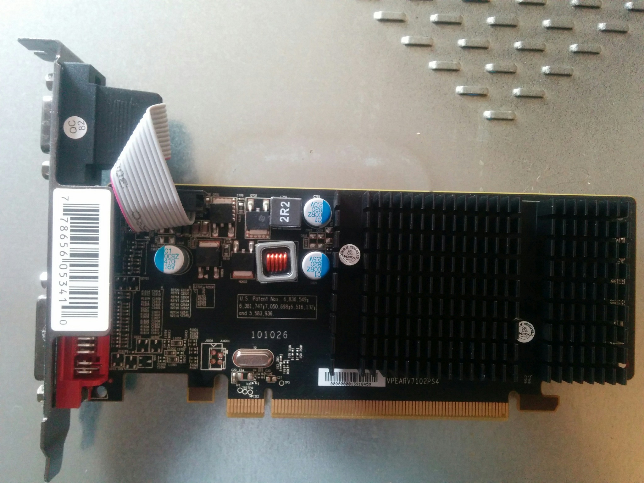
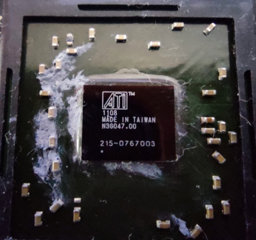
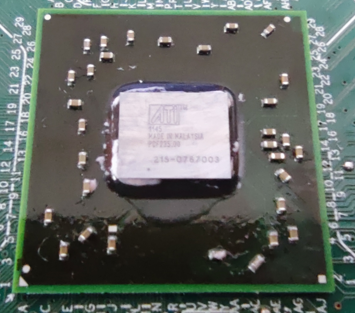
AMD Radeon HD 5450 512 MB - 2009 Here's a beauty, the slowest (and smallest, just 59 mm²) thing that could even be a Terascale2 GPU and still work. If you just wanted to add a DVI port to an older PC or a build without any onboard video, it was worth the £40 or so you'd pay. Like all AMD's Terascale 2, they could take a DVI-HDMI adapter and actually output HDMI signals, so the audio would work. It was up against Nvidia's entirely unattractive GeForce 210 and GT220, which it resoundly annihilated, but nobody was buying any of these for performance. Some of them were supplied with a low profile bracket, you could remove the VGA port (on the cable), and the rear backplane, and replace it with the low profile backplane. This XFX model was supplied with such a bracket. The 'Cedar' GPU was also featured in the FirePro 2250, FirePro 2460 MV, Radeon HD 6350, Radeon HD 7350, R5 210 and R5 220. It was pretty much awful for performance in all of these, but it was meant to be. Nobody bought one of these things expecting a powerful games machine. I dropped it in a secondary machine with a 2.5 GHz Athlon X2, and ran an old benchmark (Aquamark 3) on it. It scored roughly the same as a Radeon 9700 from 2003, despite the shader array being three times faster, the textured pixel rate is very similar, and the memory bandwidth much less. This particular unit uses RAM far below AMD's specification of 800 MHz, instead using common DDR3-1333 chips. In this case, Nanya elixir N2CB51H80AN-CG parts rated for 667 MHz operation, but it clocked them at 533 MHz (1067 MHz DDR). I got about 700 MHz out of them, 715 MHz was too far and my first attempts at 800 MHz (before I knew exactly which RAM parts were in use) were an instant display corruption, Windows 10 TDR loop and eventual crash. Being passive, the GPU couldn't go very far. I had it up to 670 MHz (11.2 GB/s) without any issues, but I doubt it'd make 700 MHz. It finally retired in 2023, after running in the server that powers hattix.co.uk, and it was part of the reason for the retirement. The server had become a CCTV DVR for its heaviest workload, and was running two Xeon E5-2640s, which it never got good use out of. The GPU was not capable of H.264 encoding in hardware, AMD did have encoding acceleration in OpenCL, but this GPU was far incapable of that. The Xeons had no hardware encoding, so had to run software encoding. The decoder would work in hardware, but recording the streams to disk meant re-encoding, and this caused a constant background CPU load on one core. This raised power use... Replacing the whole thing with a Core i5 3570K got Intel QuickSync hardware decoding and encoding. Back to the card, I'm sure XFX would say the RAM was below spec and even underclocked for power reasons, but DDR3 uses practically no power and the RAM chips aren't touching the heatsinks anyway. AMD's official (if confused) specs gave RAM on this card as "400 MHz DDR2 or 800 MHz DDR3". AMD also specifies the bandwidth for DDR3 as 12.8 GB/s, which is matched by 64 bit DDR3-1600. The 8 GB/s of this card is far below that spec. Even the memory's rated DDR3-1333 is still only 10.6 GB/s. Memory hijinks aside, all 5450s ran at 650 MHz, seemingly without exception. What rubs is that Cedar spends 292 million transistors on being around as fast as the 107 million in the R300. It does do more, has quadruple the RAM (if less than a third of the bandwidth), and has Shader Model 5.0, DirectX 11.2 compliance, and three to four times the raw shader throughput, but pixel throughput is around the same, and so is comparable performance. Sample Benchmark Results Unigine Valley (Basic, 1280x720): 226 Core: 4 ROPs, 4 TMUs, 650MHz (2.6 billion texels per second, 2.6 billion pixels per second) RAM: 64 bit DDR3, 533MHz, 8,528MB/s Shader: 1x Unified shader 5.0 (80 units) MADD GFLOPS: 104 | ||||||||||||||||||||||||||||||||||||||||||||||||||||||||||||||||||||||||||||||||||||||||||||||||||||||
|
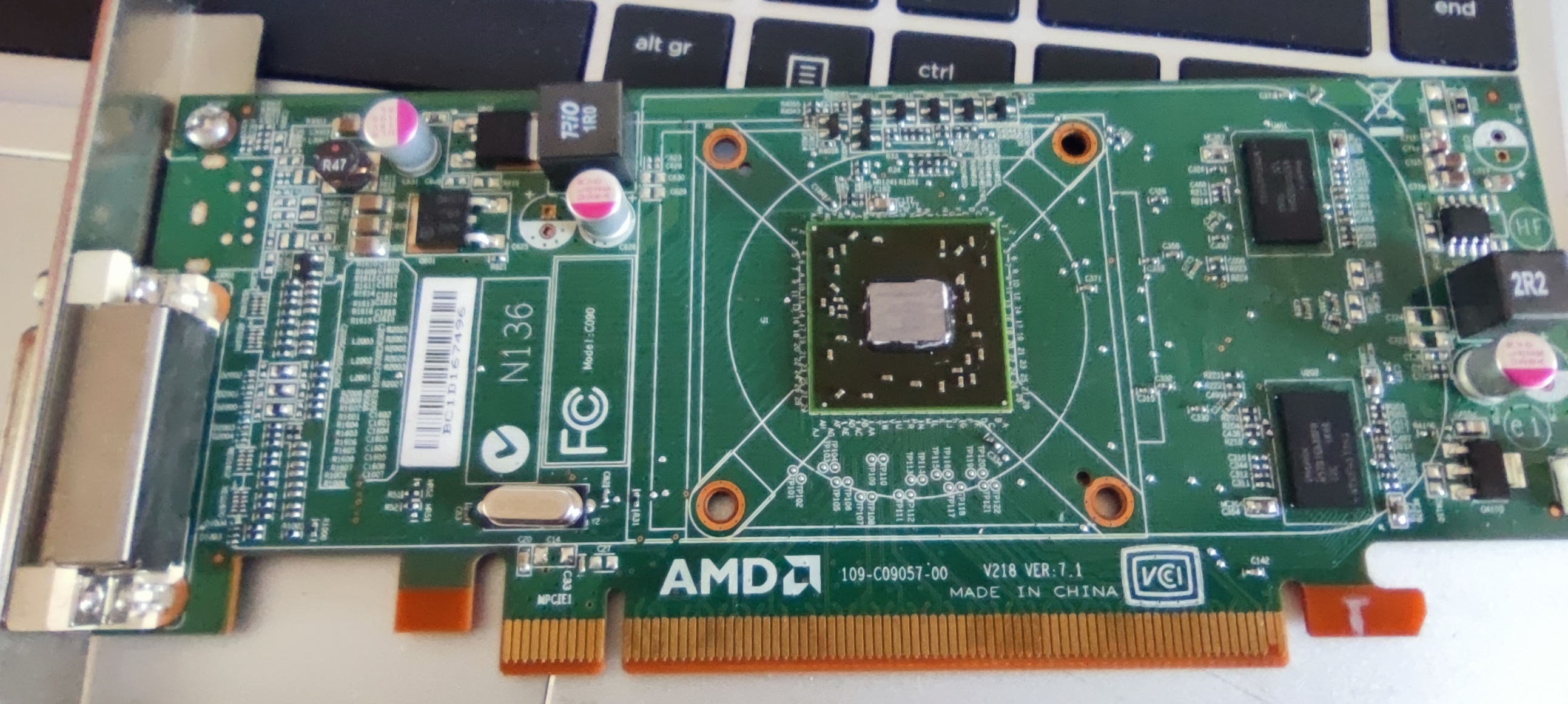
AMD Radeon HD 5450 512 MB - 2009 Here's a quandry. This is the Dell-branded AMD V218. Install it and it identifies as Radeon HD 5450 and it even went into CrossfireX with the XFX card above. The XFX 5450 above uses a 1108 date code (week 08, 2011) and this one has a 1145 date code. They're both 215-0767003 part codes, corresponds to ATI Cedar. They both clock their GPUs at 650 MHz and both run 512 MB DDR3 SDRAM. Both identify as PCI device 1002-68F9. So, they're identical, right? Not so fast! The XFX runs 533 MHz DDR3, the Dell runs 800 MHz DDR3. A small change, of course, but important when the memory bus is so cramped to begin with. It's a lot more bandwidth, 12.8 GB/s vs 8.5 GB/s. The card also uses the same BIOS as the Dell Radeon HD 6350. We've mentioned how AMD's official spec is 512 MB, 64 bit DDR3 @ 800 MHz, but it's surprising how few cards actually ran this. The Dell one here is bang on, but so many other versions were out there. Asus made a 2 GB model which ran its RAM at 450 MHz, it'd be slower than this one despite four times the RAM. XFX made a "ONE HD 5450" model which ran 400 MHz RAM. There were 400, 450, 533, 650, 667 and 800 MHz variations. You wanted faster, not bigger, so this 512 MB version at 800 MHz was one of the fastest. AMD's high volume OEM parts retained a standard heatsink fitting for many generations. This was wholly and entirely compatible with the heatsink design used on the HD 3450 just above, despite actually coming with a much smaller heatsink (TDP here was 19 watts, a HD 3450 ran 25 watts). So, of course, I swapped 'em. This one spent its entire life running two 50" 720p-ish monitors mounted to a wall in an IT ops office, typically showing SolarWinds displays, which began in around 2012 and went on to 2021 when it was retired and, somewhat unnecessarily, added to the Dell Precision T5600 which was running this server, to partner the XFX Radeon HD 5450 which was already there. After a quick shakedown, it was showing minor graphical corruption, horizontal red lines, and crashed the system. This was likely static damage to the RAM chips, so it went in the Big Box of No Escape. Sample Benchmark Results Unigine Valley (Basic, 1280x720): 254 Core: 4 ROPs, 4 TMUs, 650MHz (2.6 billion texels per second, 2.6 billion pixels per second) RAM: 64 bit DDR3, 800 MHz, 12,800 MB/s Shader: 1x Unified shader 5.0 (80 units) MADD GFLOPS: 104 | ||||||||||||||||||||||||||||||||||||||||||||||||||||||||||||||||||||||||||||||||||||||||||||||||||||||
|
TBC |
AMD Radeon HD 5750 - 2009 AMD's Radeon HD 5700 series rapidly became the mid-range GPUs to rule them. Represented by the Juniper GPU, it sported a teraflops of shader power and over 70GB/s of raw bandwidth. The 5750 promised to be the king of overclockability, being the same Juniper GPU as the 5770, with one shader pipeline disabled and clocked 150 MHz lower, but supplied with an identical heatsink on largely identical PCBs. So it'd produce less power per clock and would overclock further, right? Wrong. AMD artificially limited overclocking on Juniper-PRO (as the 5750 was known) to 850 MHz and even then most cards just wouldn't reach it. 5770s would hit 900 MHz, sometimes even 1 GHz from a stock clock of 850, yet the very same GPUs on the 5750 would barely pass 800 from stock of 700. This one, for example, runs into trouble at 820 MHz. Why? AMD reduced the core voltage for 5750s. Less clock means less voltage required, meaning lower power use but also lower overclocking headroom. 5750s ran very cool, very reliable, but paid the price in their headroom. You could hack the BIOS to restore the voltage scaling, but I never did on either of my cards. Juniper was so successful that AMD rather cheekily renamed them from 5750 and 5770 to 6750 and 6770. No, really, just a pure rename. A slight firmware upgrade enabled BluRay 3D support and HDMI1.4, but any moron could flash a 5750 with a 6750 BIOS and enjoy the "upgrade". Unfortunately there was no way of unlocking the disabled 4 TMUs and shader pipeline on the 5750 to turn it into a 5770, it seems they were physically "fused" off. The Stream Processors were arranged very much like the previous generation, 80 stream processors per pipeline (or "compute engine"), ten pipelines (one disabled in the 5750). Each pipeline has 16 cores, and each "core" is 5 ALUs, so our 5750 has 144 VLIW-5 processor elements. With a slightly downgraded, but more efficient and slightly more highly clocked GPU and slightly more memory bandwidth, the 5750 was that touch faster than a 4850. In places it could trade blows with a 4870 (see above). The 5xxx series really was just a fairly minor update to the earlier GPUs. Video decoding was AMD's UVD2.2, which could handle MPEG-2, MPEG-4 SP, MPEG-4 ASP, and H.264 up to 2K resolution and two streams simultaneously. This card is the Powercolor version, and the PCB is quite flexible. It is able to be configured as R84FH (Radeon HD 5770), R84FM (This 5750) and R83FM (Radeon HD 5670) - Redwood shared the same pinout as Juniper, so was compatible with the same PCBs. It also could be configured with 512 MB or 1 GB video RAM. The 512 MB versions were a touch cheaper, but much less capable. The Powercolor one (red PCB) was bought to add to an XFX I already had, so run in CrossFire. In games which it worked on, CrossFire was extremely powerful, but subject to all the issues a multi-GPU setup had, mostly in frame pacing. 
Core: 16 ROPs, 36 TMUs, 700MHz (25.2 billion texels per second, 11.2 billion pixels per second) RAM: 128 bit GDDR5, 1150MHz, 73,600MB/s (GDDR5 is dual ported, so is actually a form of QDR) Shader: 9x Unified shader 5.0 (80 units each) MADD GFLOPS: 1,008 |
||||||||||||||||||||||||||||||||||||||||||||||||||||||||||||||||||||||||||||||||||||||||||||||||||||||
|
AMD Radeon HD 5770 - 2009 The Radeon HD 5770 was about the champion of price effectiveness in 2009 on release, and for much of 2010. A cheaper video card was usually much slower, a faster one was much more expensive. The closely related 5750 was about 5-10% cheaper and 5-10% slower. AMD had planned a "Juniper-LE", to complete the "PRO" (5750) and "XT" (5770) line up, but the smaller, slower and much cheaper Redwood GPU overlapped, so the probable HD 5730 was either never released or very rare. A "Mobility Radeon HD 5730" was released, which was a Redwood equipped version of the Mobility 5770, which used GDDR3 memory instead of GDDR5. Redwood, in its full incarnation, was exactly half a Juniper. Observe:
AMD's VLIW-5 architecture clustered its stream processors in groups of five (this allows it to do a dot-product 3 in one cycle), there are 16 such groups in a "SIMD Engine" or shader pipeline. Juniper has ten such engines. Each engine has four texture mappers attached. Back to the 5770 at hand, when new it was about £130 (January 2011) and by far the apex of the price/performance curve, joined by its 5750 brother which was a tiny bit slower and a tiny bit cheaper. Video decoding was AMD's UVD2.2, which could handle MPEG-2, MPEG-4 SP, MPEG-4 ASP, and H.264 up to 2K resolution and two streams simultaneously. Core: 16 ROPs, 40 TMUs, 850MHz (34 billion texels per second, 13.6 billion pixels per second) RAM: 128 bit GDDR5, 1200MHz, 76,800MB/s (GDDR5 is dual ported, so is actually a form of QDR) Shader: 10x Unified shader 5.0 (10 VLIW-5 of 80, 800 total) MADD GFLOPS: 1,360 |
||||||||||||||||||||||||||||||||||||||||||||||||||||||||||||||||||||||||||||||||||||||||||||||||||||||
|
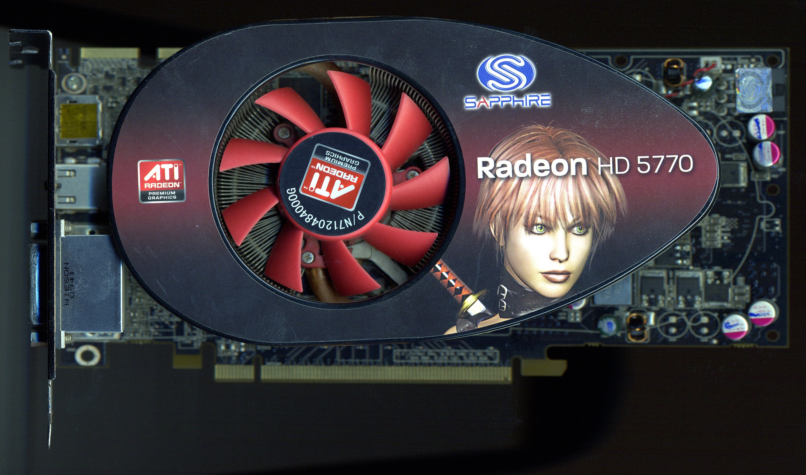
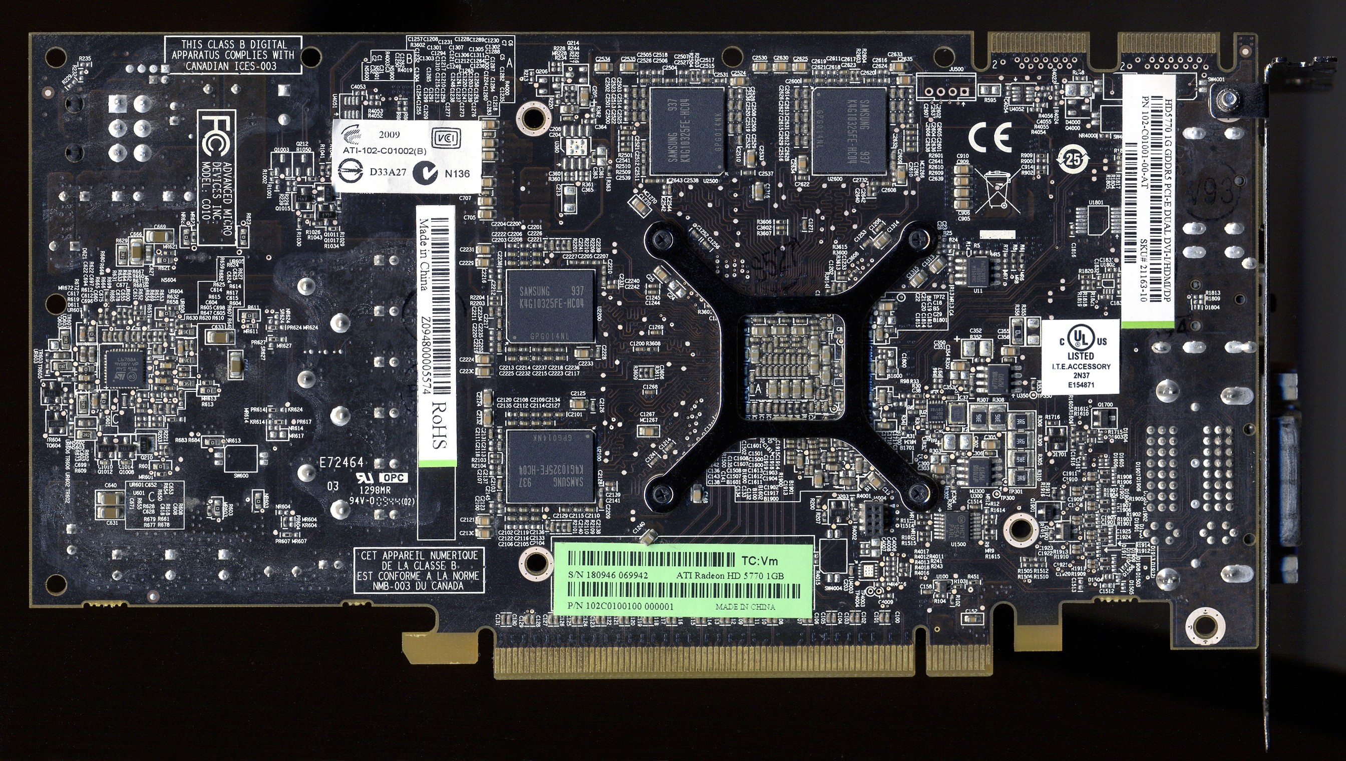
Asus EAH5770 Radeon HD 5770 CUCore - 2010 This mid-sized dual-slot design used a copper cored heatsink among its otherwise traditional radial aluminium extruded fins. The two photos here are one without the cooler and one with it, during the initial cleaning. I wasn't ever expecting to put this back into service, so I didn't really care much about the thermal interface and just dropped some unmelted phase change material back over the GPU with a razor blade. Measuring the cooler's effectiveness was to prove more complex than even that mess would make it! I can tell you the cooler this worked well, but measuring it in-situ was difficult. Let's talk about that. The AMD Evergreen driver you're most likely to use today, a late version of Catalyst 15, or an early Catalyst 16, had a very interesting bug in it. The GPU here is used mostly for its H.264 decoding ability, as the server also handles home DVR for security cameras (never farm off to a giant global megacorporation that which you can do at home) so needs to decode video streams. That, and this was the most powerful GPU I had sitting spare in the box of parts. So when the GPU is in video decoding mode, AMD applies a power profile called "UVD" after "Unified Video Decoder". This is a GPU clock of 400 MHz and RAM clock of 900 MT/s (450 MHz DDR). No matter what else you then do on the GPU, you will be in the UVD power profile! Bad when you're trying to measure its performance or maybe do some OpenCL code while the UVD is active! A fix which works on some driver versions (the permanent fix came after Evergreen went out of support) is to find HKEY_LOCAL_MACHINE\SYSTEM\CurrentControlSet\Control\Class\{4d36e968-e325-11ce-bfc1-08002be10318} in the registry, find the correct display adapter under that (it will usually be 0000, but may not be) and add a DWORD of "KMD_MaxUVDSessions" with a value of 20 hex or 32 dec. This seems to force the UVD manager into multisession mode, where clocks are managed differently. On driver version Crimson 16.1.1 Beta, this did not fix the issue. I initially figured my abuse of the thermal interface was the cause of a substantial problem: In Furmark, it hit 105C and plain stayed there, throttling back between 850 MHz and 600 MHz. I did a proper re-paste job on it to make sure that wasn't the problem. Indeed, it was not the problem. The problem was one most mid-range GPUs of that era had: They were small to medium dies (166 mm²) running at pretty high power, so were difficult to cool. This particular card had a TDP of 108 watts, but seemed to run at 125 watts under a very heavy load. They weren't power limited, they were "VDCC" limited, which was a limit on the current from the VRM. Under Furmark, it'd reach around 80% of maximum allowed... This implied the GPU could probably hit 150 watts if it were cooled well enough. So I fixed it with Bernoulli's principle. The card as supplied has a shroud around the fan and over the heatsink, removing this allows Bernoulli to work for us. When we blow air, we make a small pressure wave in front of us as that air moves other air out of its way, so also leaves a slight reduction in pressure behind it. This means we pull in a lot more air we haven't actually blown, if that air can be affected, but the shroud here stops that happening and hugely limits airflow. Removing it allows airflow to be increased by (sometimes) a factor of ten to fifteen. It's a huge effect. It brought steady-state Furmark down from 105C to 88C. This effect is also why a fan stood off from whatever it's blowing air at and (ideally) without a duct or frame will blow a lot more air than one in a duct or flush against the surface. Juniper was AMD's mainstream of this generation, with most video cards launching from October 2009 to June 2010. This hit retail in the first week of June 2010. In the UK, it would have been about £150, or £220 in January 2024 money, per the Bank of England Inflation Calculator 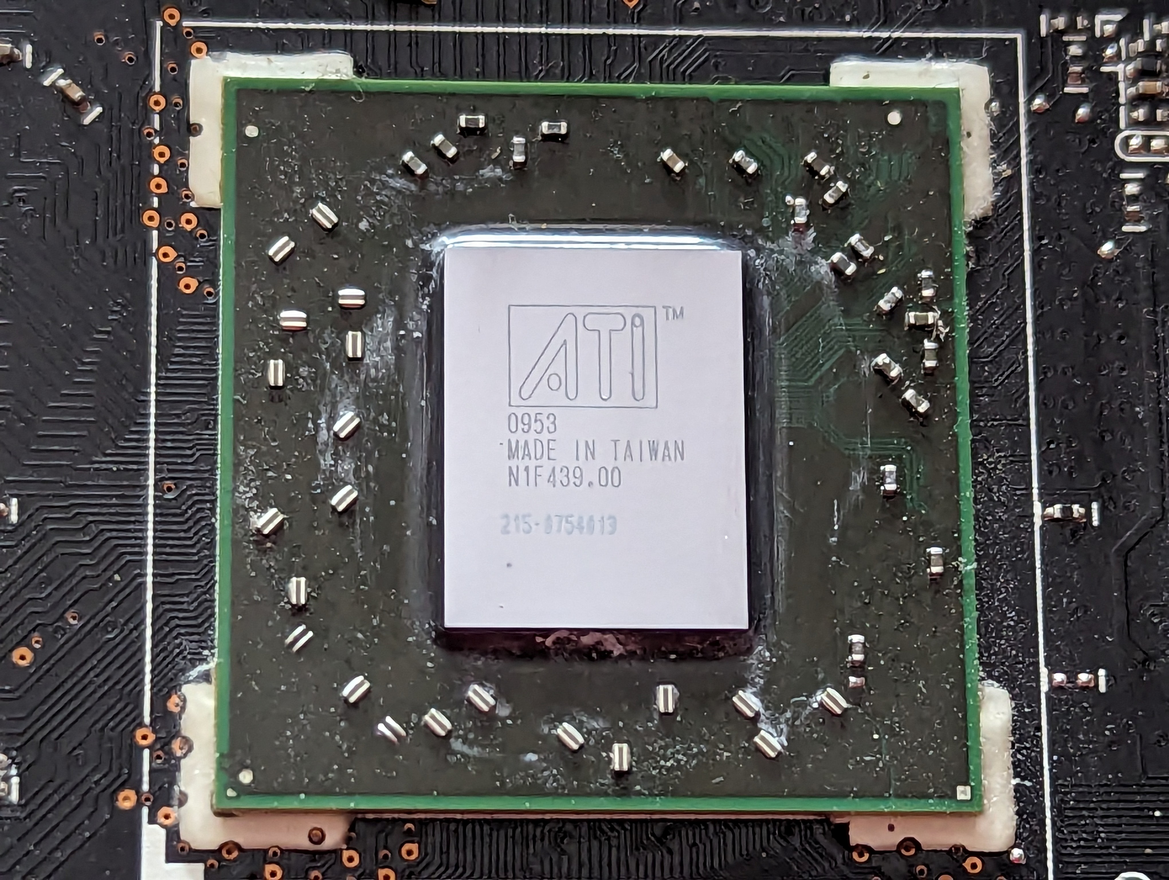
The "0953" date code shows this was made in week 53 of 2009, so probably December 30th or 31st. Now this was one step below the Radeon HD 5850, so was the upper-midrange product, roughly equivalent to the RX 7800XT or RTX 4070 Ti today. You won't find one of those at £220! As Moore's Law and Dennard Scaling died in around 2016-2019, the cost of silicon has risen enormously and prices have tripled and quadrupled to match. While AMD offered 512 MB and 1 GB VRAM options for the 5750, the 5770 was only ever officially available with 1 GB (though it could easily be designed with 512 MB). Asus used Samsung K4G10325FE-HC04 GDDR5 memory, and it's cool to decode Samsung model numbers here, so let's do that! The Hattix Samsung Memory Model Decoder The number refers to how far along the model number we are. 1 - Always K = "Samsung" 2 - 4 = "DRAM" 3 - G = "GDDR5". There's also N for graphics-intended DDR2, W for graphics-intended DDR3, and J for GDDR3 4+5 - 10 = "1G, 8K/32ms". Density and refresh. The RAM is 1 Gbit in size, and each 8K row needs refreshing every 32 ms 6+7 - 32 = "x32" DRAM organization, so this was 32 bits wide. Common widths for GDDR5 of this era were 16 and 32 8 - 5 = "16 banks" The number of banks. Other values were "4" for 8 banks, or "3" for 4 banks 9 - F = "POD_15" This is the interface, which is either POD or SSTL. POD_15 means we want 1.5V POD signalling 10 - E = "Revision", or revision 6. Samsung later expanded this as "generations" and a higher revision is not always better. Rev1 is "M" and usually qualification. Revision 2 is "A" and initial mass production. Revision 3, "B", is high performance bins. Later revisions than that usually focus on lower power or lower cost 11 - H = "170FBGA Halogen and Lead free" - the package type. GDDR5 of this generation was only available in this package 12 - C = "Commercial Normal" this is the operating conditions. This refers to temperature and power. Other options are "low" and "high", although Samsung offers segments which aren't commercial, such as radiation hardened and military, they're not usually on public spec sheets 13-14 - 04 = "0.40 ns" this is the cycle time, corresponding to a per-pin bitrate of 5.0 Gbps All this means we have four DRAMs, each 32 bits wide and 1 Gb in capacity, rated to a per-pin 5.0 Gbps bitrate. Compicating matters is that the DRAMs here are stacked, so there's another four on the back, analogous to having two DIMMs on one channel, only one can be used at any one time. So, if we ran this flat out, as seen, we have a 128 bit bus (32 x 4), each bit running at 5.0 Gbps, for a total bitrate of 640 Gbps or 80 GB/s. From our transfer rate of 1,200 MT/s (a 600 MHz clock) we calculate 76.8 GB/s, meaning this RAM is very slightly underclocked - It is rated for 1,250 MT/s. This can be explained in many ways, maybe Asus really did underclock the RAM, but more likely a 1,200 MT/s signal rate didn't neatly fit into the rating of any widely available GDDR5, and AMD/Asus wanted the headroom. Running RAM slightly slower than its maximum signalling rate means latencies can be adjusted to suit. I haven't pulled apart the BIOS to check latencies, but wouldn't be surprised to see the CAS latency set appropriately for running 1.25 GT/s memory at 1.20 GT/s. By modern standards, the Juniper-XT GPU is hopelessly outdated, even in OpenCL tasks. It has no FP64 support at all, and a peak FP32 GFLOPS of 1,360, which is usually measured to around 1,100 in benchmarks. For context, an RX 570 will usually get to around 5,200 GFLOPS, an RTX 2070 will top 9,000 and... well... even CPUs can keep up. The Xeon E5-2690 v4 (from 2015) it is being used with benchmarks to 710 GFLOPS FP32, and a completely modest Ryzen 5 5600X hits 906. This is using AIDA64's GPGPU benchmark for Single-Precision FLOPS. It isn't a rigorous test, but it is a comparable one. BIOS on these cards wasn't encrypted or signed at all, so you could load anything, including modified BIOS images. There was a simple checksum, which was there just to ensure proper programming of a new BIOS. From the factory, this had BIOS version 12.15 (with a compile date of 14th Jan 2010). It had the standard GPU and RAM clocks (850/1200), limits of 1200 MHz GPU and 1445 MT/s RAM (which no 5770 was ever going to hit), a max temperature of 109C and completely sensible performance profiles. Soft-modding was not possible on Juniper, so a 5750 could not have the additional two units enabled to turn it into a 5770. As this GPU is actually in use as of 2024, I'll get some benchmark results here at some point. That won't end embarrassingly. At least, with a Xeon E5-2490v4, we're definitely not going to be CPU limited! Core: 16 ROPs, 40 TMUs, 850MHz (34 billion texels per second, 13.6 billion pixels per second) RAM: 128 bit GDDR5, 1200MHz, 76,800MB/s Shader: 10x Unified shader 5.0 (10 VLIW-5, each VLIW-5 has 80 elements, 800 total) MADD GFLOPS: 1,360 |
||||||||||||||||||||||||||||||||||||||||||||||||||||||||||||||||||||||||||||||||||||||||||||||||||||||
|
AMD GCN The world came to a crashing halt when AMD introduced GCN. AMD's previous designs, all the way back to R520 it inherited from ATi, were VLIW-5 (with a late and minor detour to VLIW-4). "VLIW" is "Very Long Instruction Word", meaning an instruction word is a package of instruction and data. VLIW in this case is five units wide, so a VLIW-5 operation on, say, TeraScale 2, can do five FP32 operations: But has to do them all at once, and there are restrictions as to what instructions can be used together. VLIW-5 was chosen as it could single-cycle a dot-product3 lighting calculation, but real games generally ran instructions four wide, not five, so TeraScale 2's immense peak compute performance was not backed up by similarly immense game performance. Indeed, loading up TeraScale 2 with intensive operations which used the VLIW-5 design optimally would usually cause it to thermally throttle. AMD did rework TeraScale 3 to VLIW-4 in Cayman and the first APU generation (e.g. Llano, Richland), which helped efficiency somewhat. GCN is very different, it is a SIMD-16 design at core. Each GCN Compute Engine contains up to sixteen Compute Units, the diagram of a Compute Unit is shown below. 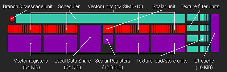 So these are four SIMD-16 units in parallel, meaning they can do four instructions at once, each instruction on sixteen FP32 values. A Wave64 wavefront presented to a CU an be viewed as a 4x64 array, where wavefronts 0 to 3 are being executed at any one time. It's best to view it clock by clock: 0. Wavefronts are dispatched. 1. Instruction 1 loads 16 values each from wavefronts 0 to 3 into all four SIMD-16s 2. Instruction 1 is completed, Instruction 2 loads 16 values from each wavefront... 3. Instruction 2 is completed, Instruction 3 loads 16 values from each wavefront... 4. Instruction 3 is completed, Instruction 4 loads 16 values from each wavefront... 5. Repeat from step 1 with newly dispatched wavefronts A GCN compute unit therefore works on four wavefronts at once, and can issue new wavefronts every four cycles. Unfortunately, if we only have one wavefront, we still block the entire four as we can only load a new one every four cycles. This means in games GCN tended to be under-utilised. Over time developers did learn to work better with GCN - They had to: GCN won the console. It was the GPU architecture of the Xbox One and PlayStation 4. If a game engine ran badly on GCN, it was a has-been engine, so there was an incredible rush by engine developers to get the best out of GCN. On release, a Radeon HD 7970 was as much as 20% slower than a GeForce GTX 680 in unfavourable cases, and in general around competitive across the board. Four years later, the GCN-based 7970 was as much as 40% faster than the GTX 680 in contemporary workloads. Games better learned how to handle GCN's one-in-four wavefront dispatch. GCN also, which wasn't exposed to begin with, had a really cool feature called asynchronous compute. This allowed compute tasks to be "slotted into" spare wavefronts. GCN had a lot of spare wavefronts! This meant AMD was aware of GCN's wavefront issue problem from the get-go, and had hardware to alleviate it. The asynchronous compute engine as finally enabled to generic software in DirectX 12. Nvidia also supported asynchronous compute, but emulated it in software. There was some benefit on the Green Team, but not as much. Nvidia primarily has less wasted capacity in a wavefront anyway. GCN initially had poor tessellation throughput. Games barely used it, so one tessellator was fine for first generation GCN (GFX6). Because this was an AMD weakness, Nvidia pushed tessellation heavily in its GameWorks middleware! In some cases, tessellation was so extreme that 32 polygons were under each pixel, dramatically slowing performance for no additional image accuracy at all. GCN's tessellation issues were mostly worked out in GFX7, Hawaii and Bonaire. Hawaii doubled the tessellators. The next enhancement to GCN was GFX8, Fiji and Tonga. Polaris (Ellesmere, Baffin and Leka) was also GFX8 level. AMD claimed a "color compression" boost, but this is GPU engineering parlance for anything which causes more effective utilisation of memory bandwidth. Larger L2s and CU prefectching added most of GFX8's advantage, where it had advantage at all. The peak of GCN was "NCE", used in Vega. Vega shipped quite badly broken, the Primitive Shader (combines vertex and pixel data for dispatch) was either broken or didn't add any performance. Vega's CU occupancy in even highly optimised games was around 50-70%, almost criminally bad, and this was the best of GCN. The Drawstream Binning Rasteriser also appeared to be non-functional, but it almost certainly did work. Vega managed a substantial improvement over Fiji, even clock corrected, despite having much less raw memory bandwidth. Like Maxwell, Vega made better use of the on-chip storage and, like Maxwell, the tile based dynamic rendering shows most benefit in bandwidth constrained situations. | |||||||||||||||||||||||||||||||||||||||||||||||||||||||||||||||||||||||||||||||||||||||||||||||||||||||
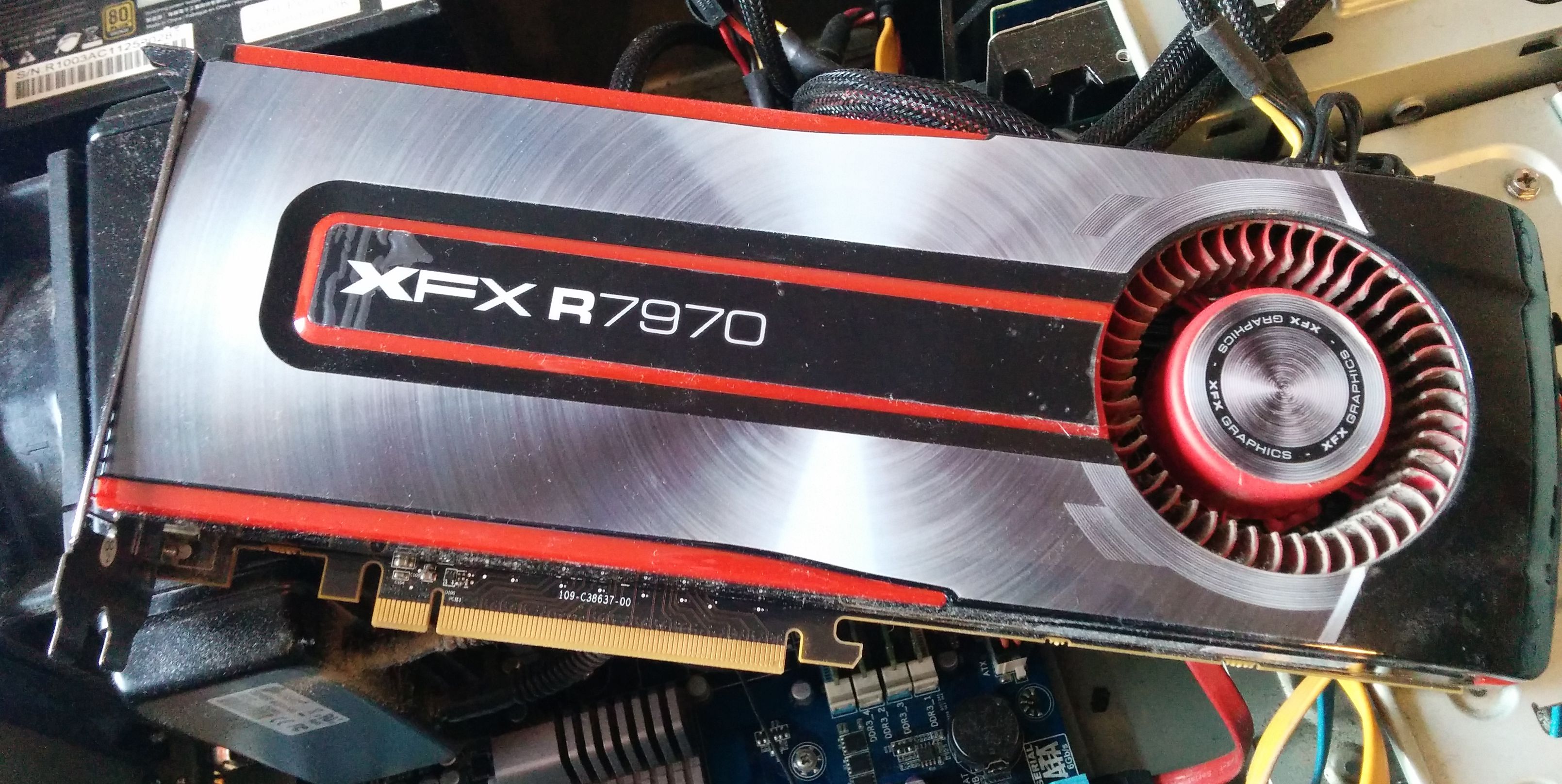 |
AMD Radeon HD 7970 - 2011 AMD's Graphics Core Next was originally a codename for what was coming after VLIW-4 (Cayman, seen in the HD 6970), the instruction set was to change from VLIW to SIMD. Each GCN "block" consists of four vector ALUs (SIMD-16) and a simple scalar unit. Each SIMD-16 unit can do 16 MADDs or FMAs per clock, so 128 operations per clock for the whole thing. The texture fetch, Z and sample units are unchanged from Terascale2/Evergreen, there are 16 texture fetch, load/store units and four texture filter units per each GCN "compute unit". AMD's Radeon HD 6000 generation had been disappointing, with rehashes of previous 5000 series GPUs in Juniper (HD 5750 and 5770 were directly renamed to 6750 and 6770) while the replacement for Redwood, Evergreen's 5 CU part, was Turks, a 6 CU part. It seemed a bit pointless. The high-end was Barts, which was actually smaller and slower than Cypress. Only the very high end, Cayman, which was a different architecture (VLIW-4 vs VLIW-5), was any highlight. AMD pulled this same stunt some years later with Polaris: If it doesn't feel it can compete at the high end, it doesn't waste resources on it. TeraScale 3 (VLIW-4, Cayman) wasn't quite ready, and Cypress wasn't enough to go up against Fermi-B, so Barts definitely wasn't. This meant AMD aimed at a solid mid-range and left the high end to Nvidia. Anyway, back to the 7970. On release, the HD 7970 was as much as 40% faster than Cayman. Such a generational improvement was almost unheard of, with 10-20% being more normal. Tahiti, the GPU in the 7970, was phenomenally powerful. Even Pitcairn, the mainstream performance GPU, was faster than everything but the very highest end of the previous generation. Over time, as games and drivers matured, Tahiti gained more and more performance. On release it was of similar performance to the GeForce GTX 680, but a few years later it was running much faster. It kept pace so well that, eventually, its 3 GB RAM became the limiting factor! Tahiti was one of those rare GPUs which takes everything else and plain beats it. It was big in every way, fast in every way, and extremely performant in every way. Notably, its double-precision floating point performance was 1/4, meaning it hit almost 1 TFLOPS of DP performance. That was still at the high end of things in 2016. UVD in Tahiti was version 3.2, which could handle the entropy decoding part of a MPEG-2 or MPEG-4 SP/ASP bitstream, so could take the unpacked bitstream from the CPU and handle the rest of it itself. H.264 was, of course, fully handled, as was VC-1 The Radeon HD 7970 was the first full implementation of the "Tahiti" GPU, which had 32 GCN compute units, organised in four clusters, clocking in at 925 MHz. This put it well ahead of Nvidia's competing Kepler architecture most of the time. An enhanced "GHz Edition" was released briefly with a 1000 MHz GPU clock (not that most 7970s wouldn't hit that), which was then renamed to R9 280X. At that point, only the R9 290 and R9 290X, which used the 44 units of AMD's "Hawaii", a year later, was any faster. This card eventually died an undignified death, beginning with hangs when under stress, then failing completely. As it was on a flaky motherboard (RAM issues), I assumed the motherboard had died, and replaced it with a spare Dell I got from the junk pile at work (Dell Optiplex 790). This video card couldn't fit that motherboard due to SATA port placement, only when a PCIe SATA controller arrived did the GPU's failure become apparent. It was likely an issue on the video card's power converters and the Tahiti GPU remains fully working on a PCB unable to properly power it. One last note on these. When cryptocurrency first became a thing, Tahiti was by far the most effective way of mining it. In 2012, you could mine Bitcoin on this GPU and run at a profit, even at the very low prices of Bitcoin back then. If you did it for, say, six months in 2012, you'd have probably ended up with two or three entire Bitcoins. The Scrypt based coins in 2013, intended to be too memory intensive for ASIC miners, could give you $10 (USD) per day in profit. Tahiti's enormous (for the time) memory bandwidth also lent it well for mining ZCash (it would do about 280-290 hashes per second), as ZCash was heavily memory bandwidth reliant. The 264 GB/s of Tahiti was above everything else which was widely available. Hawaii (R9 290/290X and their 300-series renames) was faster, but also much, much more expensive and harder to obtain. Fiji was also faster, but also very expensive and hard to buy. For cryptomining, Nvidia had nothing in that day. GTX 680 ran at 3409 GFLOPS and had 192 GB/s bandwidth, for example. Core: 32 ROPs, 128 TMUs, 925 MHz RAM: 384 bit GDDR5, 1375 MHz, 264,000MB/s (GDDR5 is dual ported, so is actually a form of QDR) Shader: 32x Unified shader 6.5 (32 GCN blocks in 4x8 configuration - 2048 individual shaders) MADD GFLOPS: 3,790 |
||||||||||||||||||||||||||||||||||||||||||||||||||||||||||||||||||||||||||||||||||||||||||||||||||||||
 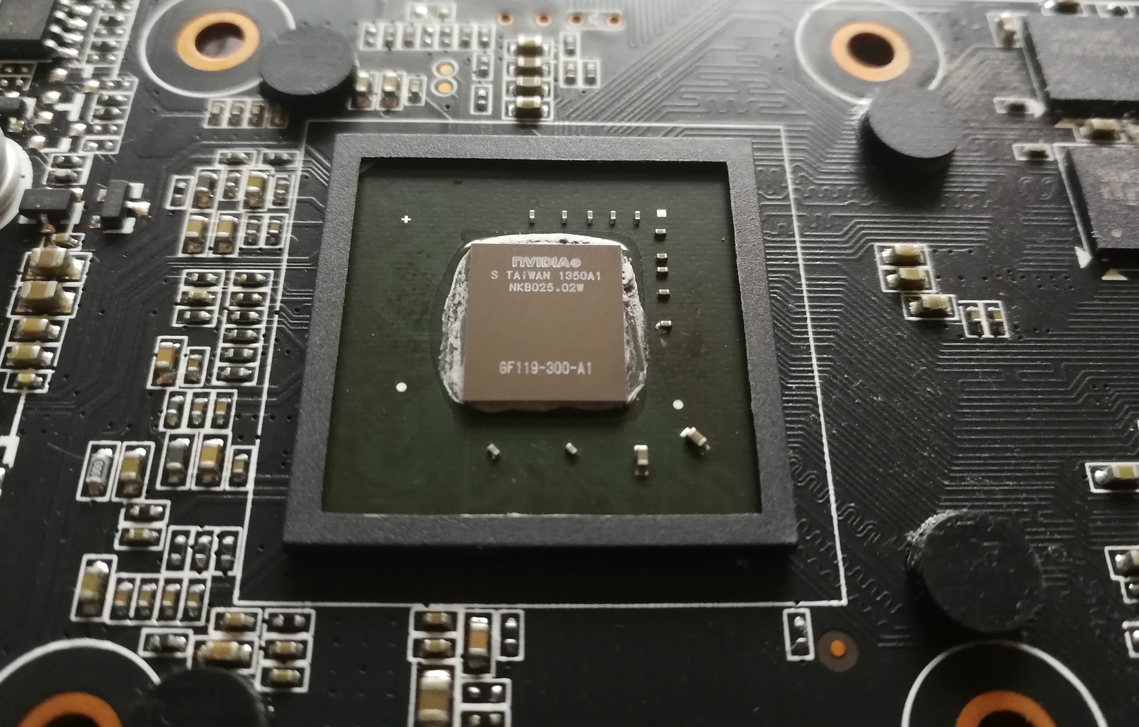 |
Zotac GeForce GT620 1GB DDR3 - 2012
This bears a sticker on the rear telling us it was manufactured in 2014, at which point the GF119 GPU was three years old. It has debuted as a low end part of the GeForce 500 series, in GeForce 510 and GeForce 520. The GeForce 620 retail normally used the GF108 GPU (even older, and first appeared in the GeForce 430), but OEM parts were GF119. This was a relabel of the GeForce 520 and used to meet OEM lifetime requirements. The provenance of this particular card is not well known: It arrived non-functional in an off-the-shelf PC which had onboard video (GeForce 7100) as part of its nForce 630i chipset, so clearly was not part of that PC when it shipped. It used the old Fermi architecture and only one compute unit of it, giving it just 48 CUDA cores. The GPU clock ran at 810 MHz (the CUDA cores in Tesla and Fermi were double-pumped) and DDR3 ran at 900 MHz over a 64 bit bus, all reference specs, as this card doesn't show up on the bus. In a system which could keep the IGP running with a video card present, the GT620 actually appeared on the bus and could be queried. It turned out to be a Zotac card with an 810 MHz GPU clock and 700 MHz DDR3 clock. No display output was functional of the HDMI and DVI present. The header for a VGA output was fitted, but the actual port was not. In later testing, the GT620 was found to be fully functional. Most likely some manner of incompatibility with BIOS or bad BIOS IGP settings caused it. The system it was in had lost its CMOS config due to a failed motherboard battery. The GeForce GT620 was very cheap, very low end, and very slow. It would handle basic games at low resolutions, such as 1280x720, but details had to be kept in check. In tests, it was about as fast as a Core i5 3570K's IGP and around 30% better than the Core i5 3470's lesser IGP. Given they were contemporaries, one wondered exactly who Nvidia was selling the GeForce GT620 to. The GeForce GT520's life did not end with the GT620. It had one more outing as the GeForce GT705, clocked up a little to 873 MHz. Its contemporary in the bargain basement was AMD's Radeon HD 5450 and its many relabels (6350, 7350, R5 220), which it more or less equal to. Core: 4 ROPs, 8 TMUs, 810 MHz RAM: 64 bit DDR3, 700 MHz, 11.2GB/s Shader: 1x Unified shader 5.1 (1 Fermi block - 48 individual shaders) MADD GFLOPS: 155.5 |
||||||||||||||||||||||||||||||||||||||||||||||||||||||||||||||||||||||||||||||||||||||||||||||||||||||
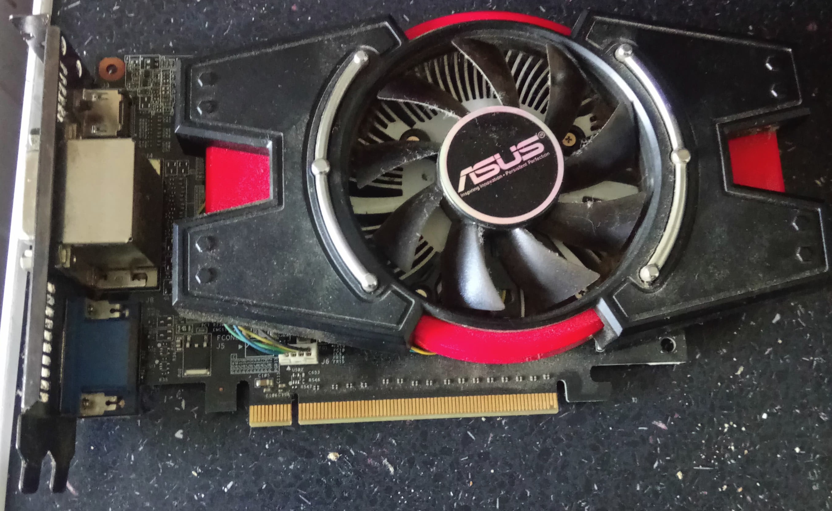  |
Asus GT640 2 GB DDR3 - 2012
This large, imposing thing is actually Asus' GeForce GT640. What could possibly need such a large cooler? Not the GT640, that's for sure. The DDR3 version used Nvidia's GK107 GPU with two Kepler units, for 384 cores, but also 16 ROPs. The DDR3 held it back substantially, with the RAM clock at 854 MHz, the 128 bit bus could only deliver 28.5 GB/s. The GPU itself ran at 901 MHz on this card. Asus ran the RAM a little slower than usual, which was 892 MHz for most GT640s. GK107 was also used in the GTX 650, which ran the GPU at 1058 MHz, 20% faster, and used GDDR5 memory to give 3.5x the memory performance of the GT640. It was around 30% faster in the real world. It, along with the surprisingly effective (but limited availability) GTX645, was the highlight of Nvidia's mid-range. The GT640, however, was not. GT640 was among the fastest of Nvidia's entry level "GT" series and did a perfectly passable job. Rear connectors were HDMI, 2x DVI and VGA. It could use all four at once. At the entry level, performance slides off much quicker than retail price does, and while GT640 was near the top of it, it was still much less cost-effective than GT650 was. The very top, GTX680, was also very cost-ineffective. The low end and high end of any generation typically have similar cost to performance ratios, the low end because performance tanks for little savings, and the high end because performance inches up for a large extra cost. RAM: 128 bit DDR3, 854 MHz, 27,328 MB/s Shader: 2x Unified shader 6.4 (2 Kepler blocks - 384 individual shaders) MADD GFLOPS: 691.2 |
||||||||||||||||||||||||||||||||||||||||||||||||||||||||||||||||||||||||||||||||||||||||||||||||||||||
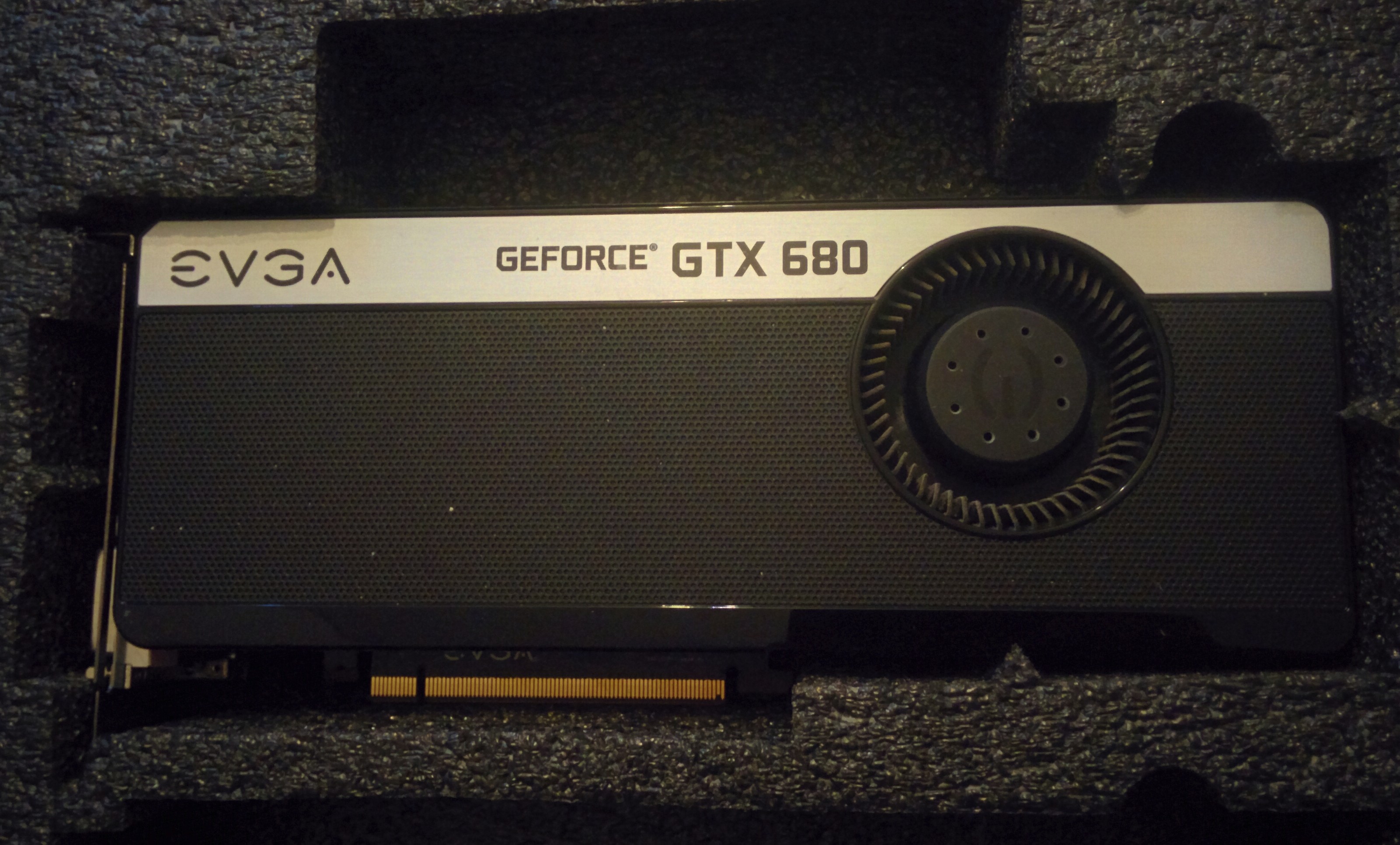 |
EVGA GeForce GTX 680 SuperClocked Signature 2 GB - 2012 The GTX 680 was the Kepler architecture's introductory flagship. It used the GK104 GPU, which had eight Kepler SMX units (each unit had 192 ALUs, or "CUDA cores"), each SMX having 16 TMUs attached and the whole thing having 32 ROPs. Memory controllers were tied to ROPs, each cluster of four ROPs having a 32-bit link to a crossbar shared among four ROPs, so each crossbar memory controller, which served 8 ROPs, had a 32 bit memory channel to RAM. With 32 ROPs, GTX 680's GK104 had 256 bit wide memory. Kepler appeared to have been taken by surprise by AMD's GCN, but just about managed to keep up. As games progressed, however, GK104's performance against the neck-and-neck Radeon HD 7970 began to suffer. In more modern titles, the Tahiti GPU can be between 15 and 30% faster. Nvidia's Kepler line-up was less rational than AMD's GCN or TeraScale 2, but still covered most of the market: GK107 had 2 units GK106 had 5 units GK104 had 8 units Nvidia disabled units to make the single unit GK107 in GT630 DDR3 and the three unit GK106 in GTX645. The second generation of Kepler, in (some) Geforce 700s added GK110 with 15 units, Nvidia pulled out all the stops to take on GCN, and more or less succeeded. There was also a "third" generation to Kepler, though this was really the second generation, it was the same feature level as GK110. GK208 was a tiny little thing, it had 2 SMX and was an almost like-for-like replacement of GK107. It cut off the NVENC video encoder and raised CUDA capability to 3.5, but also repackaged the ASIC from a 908 pin BGA to a 595 pin BGA, by cutting off half the memory width, it was reduced from 128 bits to 64 bits. GK208 was the most cut down thing which could even call itself Kepler: The smallest a Raster Engine could be was two SMXs! GK210, however, was something special. It was a third generation to Kepler, had 15 SMXs, raised CUDA to 3.7 and had a 384 bit memory bus. The five GPCs of GK210 (each with three SMXs) meant it could output 8x5 = 40 pixels per clock, but had 48 ROPs, so eight of the ROPS were always going to be underutilised, just like in GK110, which it was a fairly minor revision of. GK210 was only exclusively used in the Tesla K80, though it may have been used in some GTX TITAN and GTX 780 Ti cards. They were pin-compatible in BGA-2152 format. We're getting ahead of ourselves. GTX 680 was released into a world where AMD's Tahiti, as Radeon HD 7970, was owning everything, in everything. How did GTX 680 fare? Surprisingly well. Kepler was designed as the ultimate DirectX 11 machine and it lived up to this... These days, however, by showing how badly it has aged. While the 7970 kept up with modern games - it was still quite potent well into 2020, limited mostly by its 3 GB RAM, the GTX 680 tended not to maintain its place in the lineup. The newer the game, the more the 7970 beats the GTX 680 by, even if we don't hit the limits of 2 GB. Sample Benchmark Results Luxmark 3.1 (Hotel): 928 Unigine Valley (Basic, 1280x720): 3,450 Unigine Heaven (Extreme, 1600x900): 1,227 Unigine Heaven (Extreme HD, 1920x1080): 1,910 Unigine Superposition (1080p Medium): 6,118 Core: 32 ROPs, 128 TMUs, 1150 MHz RAM: 256 bit GDDR5, 1552 MHz, 198,656MB/s Shader: 8x Unified shader 6.4 (8 Kepler SMX - 1536 individual shaders) MADD GFLOPS: 3,532 |
||||||||||||||||||||||||||||||||||||||||||||||||||||||||||||||||||||||||||||||||||||||||||||||||||||||
 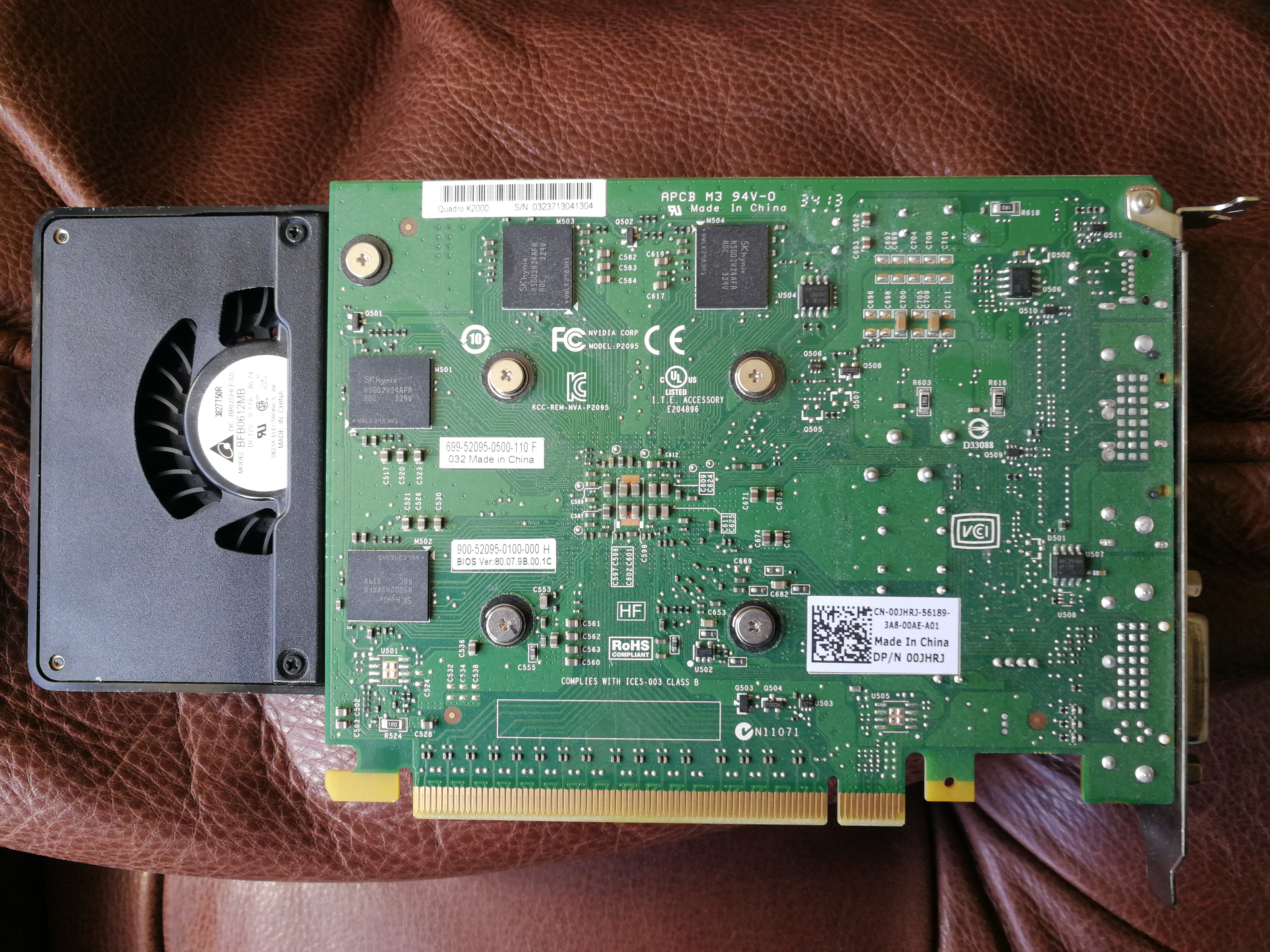 |
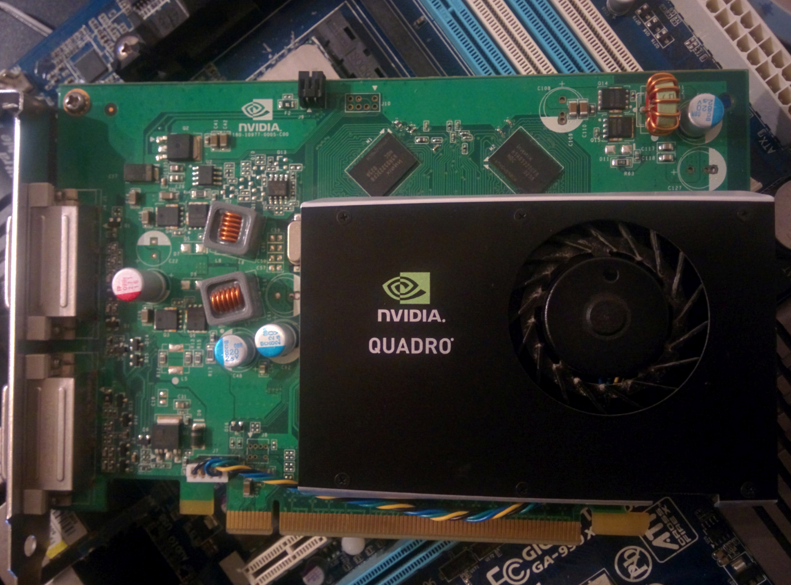
Nvidia Quadro K2000 2 GB GDDR5 - 2013 The Quadro K2000 was Nvidia's "mainstream" professional video card at $599 on launch in 2013. It is based around the Nvidia GK107 GPU, which has three Kepler blocks on it, each of which contains 192 CUDA cores (256 functional units including the very limited-use special function unit), giving 384 shader units on this GPU. Practically, it's a GeForce GTX 650 with double the memory and lower clocks. The memory on this professional card is not ECC protected and provided by commodity SK Hynix, part H5GQ2GH24AFR-R0C. Most GTX 650s (and the GT740 / GT745 based on it) used double slot coolers, while this uses a single slot design. The GTX 645 used almost the exact same PCB layout as the Quadro K2000, but the more capable GK106 GPU. The GTX 650 used a slightly different PCB, but also needed an additional power cable. Nvidia put Kepler's enhanced power management to good use on the K2000, and, in testing, it was found to throttle back quite rapidly when running tight CUDA code, the kind of thing a Quadro is intended to do. When processing 1.2 GBs worth of data through a CUDA FFT algorithm, the card had clocked back as far as 840 MHz, losing over 10% of its performance. It stayed within its somewhat anaemic 51 watt power budget and reached only 74C temperature. Professionals wanting more performance than a $150 gaming GPU should have probably bought a GTX 680 a few months earlier with the money, and had enough left over to get some pizzas in for the office. Professionals wanting certified drivers for Bentley or Autodesk products should note that both AMD and Nvidia's mainstream cards and drivers are certified. This came out of a Dell Precision T5600 workstation, where video was handled by two Quadro K2000s (GTX 650 alike, $599) to give similar performance to a single Quadro K4000 (sub-GTX 660 $1,269). By the time it arrived here, one of the K2000s was missing and the remaining one was quickly donated to a friend. The K4000 was probably the better choice, but that's not what we're here for. Core: 16 ROPs, 32 TMUs, 954 MHz RAM: 128 bit GDDR5, 1000 MHz, 64,000 MB/s Shader: 3x Unified Shader 6.4 (3 Kepler SMX - 384 individual shaders) MADD GFLOPS: 732.7 |
||||||||||||||||||||||||||||||||||||||||||||||||||||||||||||||||||||||||||||||||||||||||||||||||||||||
|
MSI GTX 970 Gaming 4 GB - 2014 "Gaming" for the 900 generation was MSI's mainstream, there's really nothing special here. Clocks are up a little compared to reference, but not enough to be worth talking about. Power in is PCIe 8 pin and PCIe 6 pin, it will not work with two six pins (even if they are sensed for 125 watts each). MSI sets a power target of 200 watts and a limit of 220 watts in BIOS. This higher power limit wasn't unusual for a GTX 970. In my testing, the GPU didn't go much above 150 watts. MSI's "Twin Frozr" cooler comes from the time when anything ending in "-r" lost its last vowel (Twitter was originally Twittr, Tumblr, Flickr, etc.) and is a very competent cooler, five heatpipes do a laudable job of moving heat from the large GM204 die. VRMs are 6 phases for the GPU and two double-output phases for the RAM controlled by a common OnSemi NCP81174 PWM controller, also used by the GTX 980s (at least reference designs) which was designed for low cost, so doesn't have an I²C interface for monitoring of power delivery. Memory is Samsung K4G51325FC-HC28, so GDDR5, 512 Mbit, 32 bits, 16 banks, 0.28 ns cycle time (7.1 Gbps per pin). The GPU is the GM204, the revised Maxwell, and made on TSMC's 28HPM process, it throws 5.2 billion features in its 398 mm² area. 
The top level organisation of GM204 is the Graphic Processing Cluster (GPC), just like Kepler. Each GPC has four streaming multiprocessors (SMs), and each SM contains four execution units, each eight-wide, and each having their own instruction buffer, warp scheduler, and dual-dispatch units. A single execution lane is SIMD-128 and made of four FP32 "cores". The four FP32 cores are joined by a load/store unit and a special function unit on each lane. Now we have a basic understanding of GM204's organisation, we know it has 16 total SMMs. A logical way to partition this is to disable a single GPC, dropping it to 12 SMMs... Nvidia instead chose to drop it to 13 SMMs. In itself, this is not a problem, and would not be a problem. What else Nvidia did, possibly driven by Maxwell's architecture, possibly a completely brainless decision, was cut the ROPs (render output pipelines) from 64 to 56. Each block of 8 ROPs is linked to its own segment of L2 cache. In GM204's specs, Nvidia was very misleading about this, and it took microbenchmarking to reveal GM204's real architecture. We'll talk about the real architecture, not Nvidia's marketing, exclusively. Nvidia said GTX 970 had four 64 bit memory controllers. It does not, it has eight 32 bit memory controllers. This is important, keep it in mind! Each memory controller is hosted by a 256 kB L2 cache. The L2 cache is linked up to a coherency crossbar. This crossbar keeps track of what's in L2 cache so each functional unit doesn't try going out to RAM to access data already cached, and memory changed by one unit can be referenced by another without the "old" data in RAM being touched. Cache coherency is well documented across the Internet, we won't rehash it all here, so the L2 TLBs (transaction look-aside buffers) are in the crossbar. Nvidia disabled one of the 256 kB L2 segments in GTX 970. From what we know already, this means that the memory controller attached to that L2 segment is uncached. This means it is non-coherent. That is, if anything accesses memory on that controller all other memory accesses have to stop. Nvidia's SVP of GPU Engineering, Jonah Alben, relased a diagram showing this, but this was also deceptive. It showed the last memory controller being a client of the L2 cache of the memory controller next to it. This was a lie! This memory controller was not a client of anyL2 cache, it went straight to the crossbar. While the data path did go through the L2 cache, it wasn't a client of it, it bypassed L2 and it is better to show it going directly to the crossbar. Alben also stated memory bandwidth remained at 224 GB/s, as it can be reached when "memory is accessed in both pools". This was also incredibly deceptive, in fact, it was an outright lie. When the uncached memory was being accessed, every other memory channel was blocked to maintain coherency. If coherency was breached, the GPU would no longer know what was in memory anywhere and would have no choice but to halt all execution - it would crash. For a machine which can run, at peak, 272 hardware threads, having the entire of memory held up by a single 32 bit uncached non-coherent memory channel is absolutely unacceptable. It would completely destroy performance, the GTX 970 would run slower than a GTX 960. This was, of course, unacceptable. So Nvidia's drivers simply didn't use that memory. If you loaded up a demanding game using DX10 or DX11 virtualised video memory, you would see around 3,500 MB in use. Nvidia was still releasing drivers with "coherency updates" some ten months after GTX 970's launch. These were thought to be hints to the driver on when it was and wasn't safe to use the non-coherent memory. My speculation is that, not long before release, Nvidia realised GTX 970 was far too close to GTX 980 (which cost 40% more) and it was in danger of making the GTX 980 irrelevant, so a last minute decision to cut back the L2 cache was made, which didn't have time to be properly accounted for. This became a massive controversy at the time. Nvidia had lied about ROP count in its guidance to reviewers (suggesting this was a last-minute decision, or someone didn't understand what Maxwell's architecture would mandate if a segment of L2 cache was disabled), lied about memory performance, doubled down on both lies, then partially came clean, but included two more lies while doing so. Finally, about eight months after launch, Nvidia admitted the 512 MB memory segment on the GTX 970 was uncached and, therefore, non-coherent. Why not come clean immediately? To do so would have resulted in everyone referring to it as a 3.5 GB product. Non-coherent memory might as well not exist, using it severely harms performance. In the end drivers in DX 11 and earlier would use it as a buffer before evicting pages to system RAM, it was a kind of L3 victim cache. In DX 12, drivers plain would not use it at all unless they absolutely had to. What a mess! Anyway, the difference between 3.5 GB and 4 GB in 2014 was almost nothing. People were more upset about the lies and Nvidia's really hamfisted way of responding to it. Its performance for its price was very competitive, slightly edging out the previous generation's massive GTX 780 Ti in some tests, and being edged out by it in others. AMD's equally huge R9 290X was usually lagging by quite a lot. In intensive games, it could double the performance of the GTX 680 which this GTX 970 replaced... in 2025! The son's gaming PC was due a rebuild and he's not terribly demanding, so the first component was this GTX 970. It was only £55, so an impulse buy, even if that was a bit steep. Raw specs aren't much over the GTX 680. In some cases it even lags. Sample Benchmark Results Unigine Heaven (Extreme, 1600x900): 1,773 Unigine Valley (Extreme HD, 1920x1080): 2,292 Unigine Superposition (1080p Medium): 7,663 Unigine Superposition (1080p High): 5,518 Oh. Yeah. That's what Maxwell did. Maxwell was able to use dynamic sized tiles when rendering to fit as much as possible into the GPU's caches (which had increased a lot), it also resized the basic warp dispatch to achieve higher core occupancy. The basic configuration of Maxwell became the basis for all subsequent Nvidia GPUs, in either 128 cores per SMM or 64 cores per SMM configuration. Maxwell was Nvidia's "GCN moment" and Nvidia wouldn't make this level of change to its architecture until Ampere and Ada, even then the changes were over two generations. Core: 56 ROPs, 104 TMUs, 1178 MHz RAM: 224 bit GDDR5, 1753 MHz, 196,224 MB/s (No, we're not including the non-coherent partition) Shader: 13x Unified shader 6.7 (13 Maxwell SMM - 1,664 individual shaders) MADD GFLOPS: 3,920 |
||||||||||||||||||||||||||||||||||||||||||||||||||||||||||||||||||||||||||||||||||||||||||||||||||||||
|
Asus Strix GTX 980 DirectCI II OC - 2014 In 2025, the son's GTX 680 was overdue an update, though he didn't mind it. I found an impulse-buy GTX 970 at £55 so just bought that for him. It's the MSI Gaming one just above. Then some legend on Reddit offered me this thing for free not even a month later. Fair enough. He wouldn't even accept the cost of shipping. GTX 980 wasn't affected by the uncacheable memory issue of the GTX 970, since all 2 MB of L2 cache was enabled on the GM204 die. In fact, the entire GM204 die was enabled. GM204 had four GPC, "Graphics Processing Clusters". Each GPC had four SMMs, "Streaming Multiprocessors", and each SMM had four CUDA clusters, a "functional unit", a single functional unit, being eight four-way SIMD units, so could do the same operation on four things at once. To illustrate how highly threaded a GPU is, each CUDA cluster can have eight threads in flight at any one time. Each SMM has four of those. Each GPC has four of those and the whole GM204 chip has four of those. This is 512 hardware threads being actively executed at any one time. 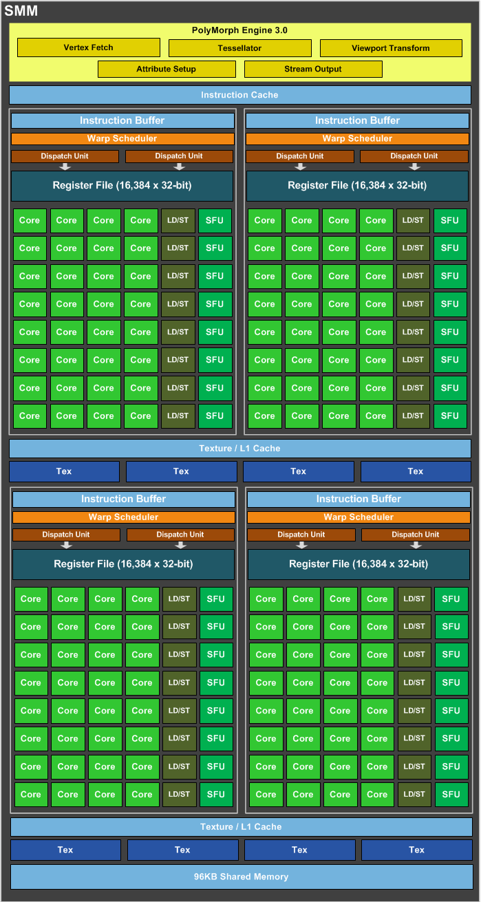
Going back to the SMM, we can see the four cores per CUDA cluster: This is misleading, as these are really ALUs. A contemporary Haswell CPU had eight "cores" in every execution engine, so a Core i7-4790K, with four CPU cores, had 32 "cores" if we counted "cores" like Nvidia does. See those rows of Core, Core, Core, Core, LD/ST, SFU? Each one of those is an "functional unit" (FU). These are eight way multithreaded inside the SMM, along with four more like them. Moving up from the functional units, we reach the dispatch units and register file. The register file is the data the cores can access without penalty, so the data arrives with the instruction. Each execution unit will be working on four 32 bit values at once, we have eight of them, so we have 128 registers being actively used at any one time. The dispatch unit controls occupancy of the registers and the FUs, but you will notice we only have two of them. This is really one dual-issue dispatch unit. This dual-issue dispatch unit can issue up to two operations per clock from a warp, a warp is eight SIMD-128 instructions. Each FU is pipelined four-deep, so can be working on (ideally) four instructions at once, but rarely would be, and would cause huge overheating if it was that heavily utilised! The scheduler and dispatcher work in concert, so we can skip up a level to the instruction cache and texture cache. Anyone familiar with CPU architecture is going to instantly recognise this as a level 1 instruction cache (L1I$) and a level 1 data cache (L1D$). They would not be wrong. Previoius Nvidia architectures had aliased L1 cache to local shared memory, but not so in Maxwell. L1D$ in GM204 is 24 kB, while L1I$ is 16 kB. The shared memory can be thought of as a small L2 cache, and most applications treat it this way. Each SMM also has eight texture units, each able to sample a single RGBA value using a programmable sample matrix. Moving out from this, we have the entire GPU. The SMM joins four more like it in the GPC, and the GPC is unified by a Raster Engine. This is what handles pixel data, and sends it out to the ROPs. 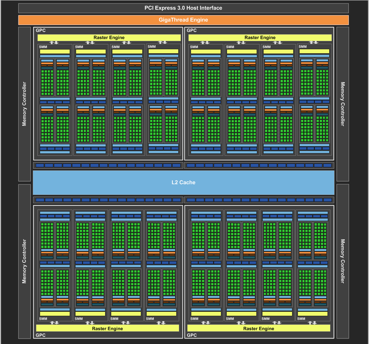
We can see blocks of four render output pipelines, ROPs, alongside the L2 cache, this is a little misleading. Each ROP is 16 pixel units (which Nvidia calls "ROPs", for historical reasons) so we can output 64 pixels per clock to L2 cache, from there the cache and crossbar handle our writing out to RAM. The ROPs are absolutely critical to Maxwell. They're very closely linked to the crossbar, so data going out back to memory always goes through a ROP, even if it is unchanged by the ROP. This is done as the crossbar enforces memory coherency via L2 tag RAM, something extremely important on a massively multithreaded architecture. After the crossbar is the L2 cache and memory controllers. These are arranged in pairs, so each "memory controller" has two segments of L2$ and each of these has one memory controller, so each 32-bit memory channel going out to DRAM (GDDR5 here) has its own 256 kB L2 cache. This L2$ is only able to cache the memory associated with its own memory controller, which is 512 MB in the GTX 980 (and GTX 970). This brings total L2$ to 2048 kB, at which point it's worth noting that GK104 in Kepler had 512 kB for the entire GPU. Each 32 bit memory controller in Kepler (which it had the same four pairs as Maxwell) had just 64 kB L2 cache. It barely did anything! The GTX 970 entry covered how tightly coupled ROPs are to L2$ segments, via the crossbar. And that's GM204 in a nutshell! It's a point of inflection in GPU design, GPUs had become so large and parallel that even their own stupidly fast "the memory is the cache" memory buses couldn't keep up, so Maxwell invested heavily in caches. Maxwell was a huge generational improvement from Kepler, even delayed by a year with TSMC's 20 nm process being limited (Maxwell was back-ported to late-generation 28 nm), that Maxwell was the first Nvidia GPU to be "truly modern", bringing Nvidia up to AMD's GCN capability levels. GM204's desktop products were the GTX 960 OEM, GTX 970, and GTX 980. The GTX 960 OEM was a little notable as it had more SMs than the standard 960 and a 192 bit memory bus, though it declocked them both to very similar (slightly more) than the standard GTX 960. Mobile GTX 980 also used the GM204, in a cut-down configuration, but with 8 GB VRAM in some models. These aged very well! Nvidia reserved 8 GB on desktop for its Quadro parts, the Quadro equivalent of a GTX 980 was the Quadro M5000. One criticism of the GTX 980 is that it has not aged well. The throughput of the GPU, 5.2 TFLOPS, puts it right next to the RX 470 from two years later or the RX 570 a year after that. Both of those, however, had common and popular 8 GB versions and remain effective low-end GPUs even in 2025. The GTX 980 would out-perform both of these if it was not limited to 4 GB VRAM and Nvidia never authorised anyone to make 8 GB versions. An engineering sample of a GTX 980 with 8 GB surfaced in 2017 and the Quadro M5000 was basically a declocked GTX 980 with 8 GB. Some mobile GTX 980M parts had 8 GB, as this was an option there. Maxwell's successor, Pascal, kept the exact same caching layout as Maxwell. GP104 Pascal reorganised the SMs into pairs behind a "texture processing cluster", TPC, something which really already existed in Maxwell, but was formalised in Pascal. TU104 in Turing built on this by putting two SMs into a TPC and doubling L2$ to 512 kB per 32-bit memory controller, this doubling of L2 cache was responsible for practically all of Turing's performance uplift, where it existed. Ampere was to further modify this by moving the ROPs into the GPCs, but disabling a ROP still took out that ROP's segment of L2$ and disabling a L2$ segment took out the ROP. This particular card wasn't stable in the kid's machine, so was replaced with the GTX 970 already mentioned but intensive stress testing in the server machine could not make it produce a fault, though it did crash a 3D benchmark (by hanging the entire machine, as it had done on the kid's PC) once. The VBIOS of the Asus Strix OC card ahd a power limit of 240 watts, which corresponded to about 185 watts on the GPU die, 40 watts on the VRAM, and about 15 watts lost in VRM conversions. At 240 watts, Asus' cooler would keep it at a comfortable 78 celsius steady-state with a hotspot touching 91 degrees. GPU clock under this full load would be about 1260-1290 MHz depending on the exact workload. Core: 64 ROPs, 128 TMUs, 1279 MHz RAM: 256 bit GDDR5, 1753 MHz, 224,400 MB/s Shader: 16x Unified shader 6.7 (16 Maxwell SMM - 2,048 individual shaders) MADD GFLOPS: 5,240 |
||||||||||||||||||||||||||||||||||||||||||||||||||||||||||||||||||||||||||||||||||||||||||||||||||||||
 |
XFX RX 570 RS XXX Edition 8 GB (RX-570P8D VC.1) - 2017 The RX 570 was announced as a rebrand of the RX 470 with slightly improved GPUs. Advances in the 14 nm FinFET process at TSMC meant the GPU controlling firmware could run them faster for longer, or at the same clocks with less power. On release, Polaris was, let's say, not great. It didn't beat Nvidia's previous generation, the 900 series, in either absolute performance or in price/performance. A GTX 970 was a better buy than an RX 480, and they were about the same price. In most tests which weren't Wolfenstein II (in which the GTX 970 did very, very poorly) the RX 480 was around 10% behind. However, AMD did not have the 900 series to beat: It had the 1000 series to beat. Price-wise, the RX 480 slipped in just below the GTX 1060 6 GB. Performance-wise, the RX 480 slipped in just below the GTX 1060 6GB. AMD's high end was the R9 Fury X, still, which was showing its age (and expense): R9 Fury X was AMD throwing everything up to and including the kitchen sink at Nvidia's GTX 980, and losing. It had HBM2, watercooling, the massive Fiji die, but was still an architectural generation behind. Polaris, then, is when AMD's GCN architecture finally became too dated to compete. AMD didn't even try to make a big one, Polaris 10/20 (this RX 570 used Polaris 20) was very much mainstream as far as GPUs went in 2016/17, a bigger Polaris might have done better, but would have fallen off the price/performance curve. AMD had already tried going big with GCN, as Hawaii and Fiji (Fiji being the fastest GCN product ever made if we discount Vega, which we probably shouldn't), embarassed itself in all but cryptomining. As 2018 drew on, AMD did an RX 590 refresh of the RX 580, with more power, more clocks, and manufacturing improvements. It didn't embarass itself next to the GTX 1660, but didn't win either. Polaris was a disappointment for Team Red. With the Polaris 20 GPU having 36 compute/vector units (each having 4 GCN SIMD-16 cores), the 32 core variant was essential for yield harvesting. If a single core was faulty, the fault could be mapped into the disabled area. In GCN, dispatch units were four wide, so logically arranged as four columns of compute units. Polaris 20 implemented 9 compute units per column (compare with Tahiti and Tonga which used 8) and they had to be symmetrical, so long as they all had the same "depth" of compute units. RX 570 disabled one unit in each column and was die fused, so they couldn't be re-enabled. This left it with 32 units active, the same as Tonga and Tahiti, being fed by its 256 bit GDDR5 bus, the same as Tonga (R9 285, R9 380, R9 380X). It behaved very much like a die-shrunk Tonga because, well, that's what it was.
A lot about Polaris was "the same as Tonga" because the GPU was, in fact, the same as Tonga. It was the same design, resynthesised for 16 nm FinFET, and given 9 compute units per dispatch block (there were four such dispatch blocks) instead of 8. Being on the smaller 16 nm process, Polaris 10/20 was only 232 square millimetres. On the older 28 nm process, Tonga was 359 square mm. Polaris had all the same technology, all the same instructions, features and capabilities as Tonga. AMD updated the video encoding/decoding IP block a little, but not massively. This is not to say Tonga was bad. It was AMD's "GFX8" technology level (which actually describes compute capability), with DX12 compliance (at the 12_0 featureset), SIMD-32 instruction set and hardware asynchronous compute. It was, however, released as a minor update to GFX7 in 2014! By 2017, GFX9 (Vega) had been released, and 2019 saw GFX10, RDNA, released. As there isn't a good list of AMD's shader ISA levels anywhere, here it is:
Polaris 10 being the biggest of the 14nm Polaris generation was perhaps appropriate. It was significantly less powerful than Hawaii of the R9 290/390 series, but still kept up with it. Its 36 units at 1.25 GHz slightly couldn't keep up with Hawaii's 44 units at 1 GHz in compute, but compute wasn't GCN's bottleneck. Its 1.75 GHz 256 bit GDDR5 memory had no hope of keeping up with Hawaii's 1.5 GHz 512 bit array. RX 580, Polaris 20 in its most optimal configuration, was a wash against R9 390X. It was also around half the price! RX 570 (and RX 470) was positioned to replace R9 380 in the market, which it had around a 30-40% advantage over. It was priced next to Nvidia's GTX 1060 3GB, which it usually slightly beat until quality settings got raised, then the 3 GB of Nvidia's card got comprehensively dismantled by AMD's 8 GB provision. The 6 GB GTX 1060 again traded blows with the RX 570 (and usually the RX 570 was on the losing side) but was significantly more expensive. Who pays more for less? AMD's position was quite obvious: Pascal, typically as GTX 1050 Ti and GTX 1060, was much more power efficient and got way, way higher performance per watt. AMD's older GCN design couldn't match that for perf/watt, but it could match it for perf/dollar. AMD pushed the RX 570 and RX 580 to the apex of the bang for buck curve. Later in its life it was up against Nvidia's GTX 1650, which it typically won against quite substantially. Nvidia's smaller Turings offered slightly more in the way of features (DirectX 12 feature level 12_1), but video cards have rarely sold on anything but performance. This particular card is based around the same PCB and cooler design as XFX's RX 580 GTS XXX Edition, but one heatpipe is missing so it doesn't quite have the same thermal capacity. XFX saw fit to give it switchable "performance" and "stealth" BIOSes which actually enabled quite a cool little trick. Perfomance clocked GPU/RAM at 1286/1750, while stealth clocked at 1100/2050. Ordinarily, of course, the RAM clocks for stealth were not available for performance, but if we set the GPU to stealth, reset the video driver to defaults, make a GPU performance profile, then change the GPU to performance BIOS, we can clock the GPU at normal levels while retaining the 2050 MHz RAM. This would knock the card a little higher than its board power should be. The "stealth" BIOS was, of course, intended for crypto-mining, it ran the RAM faster and reduced power use on the GPU core without sacrificing much performance in the kinds of workloads scrypt and eth based coins needed. This one would clock at 1351/2050 with around 95% stability. It was possible to find workloads which would go wrong at thoose clocks and we'd be thermally or power limited in games. A quick bash of The Witcher 3 had it clocking at 1275 MHz with power limit +20%. The GPU power seemed to be set at 125 W, for a 150 watt board power, raising power limit only applies to the GPU, so +20% should give 25 W extra to play with - More than the cut back cooler on the card can handle. It clocked at 1200/2050 with the GPU voltage at 0.975V, giving a dramatic power savings, at the expense of the top 10% of performance. Connectivity was handled by three DisplayPort outputs, one DVI-D, and one HDMI. There was no facility for a VGA connection. Hynix, Samsung and Micron GDDR5 were common on these cards, typically the Samsung was the fastest in terms of timings, but there wasn't a lot in it. This used Micron GDDR5 rated for 2 GHz and tRCDW-tRCDWA-tRCDR-tRCDRA-tRC-tCL-tRFC of 23-23-29-29-79-22-219. At stock 1750 MHz, it would run 21-21-26-26-70-20-192. XFX was using the same PCB (with VRAM) for all Polaris 20 parts and just adding the GPUs on later as they were binned. The Black Edition got better RX 570 GPUs which ran cooler, while the XXX got the majority of chips. XFX didn't use any high binned RX 570s, Sapphire and Power Color were the only vendors with RX 570s boosting over 1.3 GHz. Official clocks were 1168 base, 1284 boost, and 1750 RAM. AMD guaranteed a minimum clock of 1168 MHz, which was its "base clock". This is what you'd get if you met the bare minimum, put it in a cramped case with nearly no airflow, and gave it an intensive workload. This is up from the RX 470's base clock of 926 MHz, but that had to fit into a board power of 120 watts (so only 100 watts for the GPU). In nearly all cases, including every case I tested this card on, it did not drop as low as base clock, even in The Witcher 3 at "ultra" (no Hairworks) and the GPU running into thermal limits at 90C. In fact, the AMD boost clock of 1244 MHz was about the lowest observed. Right until I put it in a case designed for blower video cards, a Dell Precision T5600 workstation. They relied on positive pressure from the three intake fans to channel air, and relied on either low power video cards (2x Quadro K4000 was a good option) or on video cards doing their own exhaust. Running intensive workloads here (OCCT Furmark) got the video card throttling back to below 800 MHz! This is a pathological case, of course, and The Witcher 3 ran above 1200 MHz most of the time. In reality, nearly all RX 570s ran a boost clock of 1286 (some factory OCs ran as high as 1340), and "boost clock" really meant "the clock it will run at unless it reaches power or thermal limits". By 2020, when I bought it for £125, it was showing its age and was only good for 1080p at medium/high in most demanding games of that year. The 8 GB RAM did help: Cards with more RAM tend to age better than ones with less, even if the don't have a lot of benefit when new. In late 2020, COVID-19 shortages hit other GPUs, meaning RX 570s nad RX 580s rose a little in price, then in early 2020 was a cryptocoin mining boom again... This RX 570 hit £350. Had I wished to resell it, it would have fetched £200-250 on eBay, as the 8 GB model was suitable for Ethereum mining where the 4 GB model was not. This particular card, the XFX RX 570 RS XXX Edition was the lowest end model of RX 570, and had a very cut back design. The "RS" is used for their lowest tier, just below the "GTS" and usually alongside it. GTR and GTR-S were the higher ones. "XXX Edition" is also the lowest tier of card, with things like "MERC" or "QICK" above it. The heatsink in this case is the same one from the "XFX RX 480 RS" but has a heatpipe missing and, under load, the card runs very hot (The XFX RX 570 RS Black Edition was, to my knowledge, identical in every way but for a 1328 MHz GPU clock). At anything north of around 1330 MHz, it is thermally limited. This particular one doesn't undervolt very well either, so it's heatsink or nothing. As 2020-2022 was "nothing" then I started investigating ways to improve the cooling. Adding thermal pads to contact the backplate and small copper heatsinks to hot spots behind the VRMs on the backplate didn't really change much. With the heatpipe missing, the limitation was on how fast heat could be moved from the GPU die and just two heatpipes wasn't enough. The VRAM was also not cooled other than by wash from the fan, probably why XFX used RAM rated for 2050 MHz (8,000 MT/s) but clocked it back to only 1750 MHz. Also, XFX lied on the box. I mean, outright lies. First was deception: It showed a big multi-heatpipe cooler design as "Ghost Thermal 4.0" which was completely absent. Second was the big boxout on the back of the box saying "[Hard Swap] Interchangeable Fan" which is plain not there, the swappable fan connections were not present. This one left in an unusual way: It was sold. I traded it in for £73 in early 2023, around its third birthday. Given that the price new was £125, in 2020, and it was three years after launch then, this was effectively a six year old video card. I resold it, at retail for 58% of what I'd paid for it. It then went on sale for £110, or 88% of what I'd paid. This was how bad the video card market was in 2023. Why did it sell so well? It was the 8 GB model. Just a few pounds more to buy new over the 4 GB model, but substantially more future-proof. Reference Benchmarks at 1350/2050 (literature scores used for other GPUs)
Unigine Heaven (Extreme, 1600x900): 1,590 Unigine Valley (Basic, 1280x720): 5,541 Unigine Valley (Extreme HD, 1920x1080): 2,061 Unigine Superposition (1080p Medium): 7,645 Core: 32 ROPs, 128 TMUs, 1286 MHz RAM: 256 bit GDDR5, 1750 MHz, 224,000 MB/s Shader: 32x Unified shader 6.5 (32 GCN blocks in 4x8 configuration - 2048 individual shaders) MADD GFLOPS: 5,267 |
||||||||||||||||||||||||||||||||||||||||||||||||||||||||||||||||||||||||||||||||||||||||||||||||||||||
 |
Gigabyte Windforce 3G GeForce RTX 2070 8GB - 2018
The Turing GPUs had a little extra in them which previous GPUs lacked or, at least didn't have completely. Volta, the previous generation, was a single GPU, GV100, aimed at datacentre use and AI research use. It added an array of tensor cores, very specialised hardware for solving low-precision matrix multiplies or "tensors". They perform a multiply of two 4x4 FP16 matrices, then adds that to a third FP16 (or FP32) matrix, all as fused multiply-add. The input matrices in the multiply can also be INT8, INT4, or INT1, so they can do 1024 "bits worth" of operation per clock, so INT8 has twice the throughout of FP16. This was helpful in a lot of artificial intelligence applications, such as machine vision and machine learning as it's the bulk operation neural networks perform. However, Nvidia's core market still remained gaming, and the tensor cores did nothing for that. They were great for AI research, but this was a very small volume of sales in 2016-2020. Tensor processors were a very competitive market, but a small one. Google was in on it with its TPU, and Google was a very big fish in the small pond. Google made its TPU for its own use. It was known that most of the industry heavyweights were also working on tensor accelerators. The market was about to get very competitive, so it is rumoured that Jen-Tsun Huang, Nvidia's co-founder and CEO, demanded a gaming application or the project was going to be cancelled. Nvidia engineers soon realised that the tensor cores could do very effective de-noising and one of the limiting aspects of their RayTracing Extension (RTX) CUDA library was the sheer number of iterations needed to get noise down: They needed something like 50,000-200,000 iterations for a single frame. However, using tensor core de-noising, this could be brought down to 2,000 iterations, enough to be done almost in realtime. With a little extra help from hardware which could solve incident normals (giving the angle a line intersects a surface, used for lighting direction) and a quick way to resolve a bounding volume hierarchy (BVH), RTX could be done absolutely in realtime. Turing added RT cores (which solved incident normals and accelerated BVH) to Volta's tensor cores and RTX was promoted from being an experimental CUDA library to being a suite of semi-related technologies for shadowing, lighting, and depth testing. A similar algorithm to the tensor de-noiser could also reduce noise in image scaling and provide good quality upscaling, so a GPU could render at, say, 1600x900 and then use the tensors to upscale that to 1920x1080 with little loss of quality. Nvidia called this "Deep Learning Super-Sampling" or DLSS. Originally it was an artefact-strewn mess, but with DLSS2.0 and DLSS3.0 it became a highly useful tool to raise framerates. The "Deep Learning" bit of it refers to the use of a convolutional auto-encoder neural network which is trained on common scaling artefacts. If it finds one, it blurs it out. Turing also had Nvidia's "Boost 4.0" DVFS (dynamic voltage and frequency scaling) technology which works very much like Precision Boost Overdrive on a Ryzen CPU. If it has temperature and power margins, it will raise clocks higher to use that margin. The stock clock for an RTX 2070 is a boost of 1620 MHz and a base of 1410 MHz. This particular card wull run around 1770-1820 MHz in games by default. It'll overclock to a peak of around 2100 MHz, but won't sustain that, dropping back to 1950-2000 MHz. At this level, it is hard-hitting power limits, so I replaced its default BIOS (195 watts max) with one enabling a 240 watt limit. The RTX 2070 was the top level TU106 GPU, with all 36 SMX engines and the entire 256 bit GDDR6 controller enabled. RTX 2060 was the same TU106, but turned off a block of six SMXs and a 64 bit memory controller. Each SMX has one RT core and 8 tensor cores, so RTX 2070 had 288 tensors and 36 RTs. A year later, RTX 2070 was replaced in the market by the RTX 2060 SUPER, which disabled only two SMXs, giving nearly all the same performance at a lower price, and by the RTX 2070 SUPER which used TU104 GPUs to give 40 SMXs (TU104 had 48 in total) and so higher performance at the same price. Gigabyte's Windforce series is its basic level of video card, so has a basic cooler (two heatpipes), three rather small fans and a thermal limit of 175 watts (with a hard cap of 200 watts) while the reference card was rated to 175 watts but had a hard cap of 225 watts. Gigabyte made much of the opposite flow direction of the middle fan, which avoided shearing interactions of the adjacent fans. It does reduce noise a little, but has no measurable impact on airflow or temperatures. Counter-rotation is Gigabyte's thing, nobody else seems to use it. Power delivery on the PCB is quite good. How much do you need for a video card which is rated south of 200 watts? Actually less than this. A PCIe 6-pin connector is rated for 75 watts, the slot itself can do 75 watts, and an 8-pin can deliver 125 watts. So, just a single 8-pin and the slot can deliver 200 watts, more than enough for this card. Here we see both 6-pin and 8-pin connectors in use, meaning the peak deliverable power is 275 watts. The BIOS provided by Nvidia had a default TDP of 175W which could only be raised to 200W. There is a BIOS for this card which raises that cap to 240 watts. It's Nvidia's way: Nvidia provides the tools, you use them within approved limits. The OC Scanner as seen in EVGA Precision X, Gigabyte Aorus Master, MSI Afterburner, is an Nvidia tool. The voltage bumps they do are within Nvidia limits. Clock offsets, per Nvidia limits. The BIOS is signed and encrypted (since Pascal, though certificate checking was introduced in Maxwell) but cross-flashing (e.g. Asus to Gigabyte) is allowed. It's a kind of sandbox, a walled-garden, for minor tweaking. You won't hurt yourself here, have a play, Big Daddy Nvidia is watching over you so you don't need to worry your cute little face. Don't forget that you will never escape.. Be careful when BIOS cross-flashing, which I did to this card (to raise its max power from 200 to 240 watts). Nvidia had two lines of GPUs in the Turing family, so this one is TU-106-400. There was also, on the RTX 2070, a TU-106A-400. The "A" signified it allowed factory overclocking (irrelevant really) but also the BIOS for the "A" cards had much higher power limits, some up at 300 watts. The PCI ID for the "regular" TU106-400 was 10DE (Nvidia) and 1F02. The "A" GPU was 1F07. To be safe, the PCI ID has to match, as well as RAM type. The highest power limit I found was 240 watts, though this card seemed to be capable of more, it had some missing VRM outputs, but still enough MOSFETs to reach at least 300 watts. When raising the power, it's also important to be aware of how much power is available. This guy has the PCIe slot, 8-pin and 6-pin. Together, these add up to 75 + 125 + 75 respectively, so 275 watts. You wouldn't usually want to go over this, though a 6-pin made as a 6+2 is much meatier and can handle 82 watts (since the per-pin rating of an 8-pin is higher than a 6-pin) and most good PSUs use a tighter version of the specification, as defined by Intel, to allow even higher powers. Overclocking these, at a basic level, is simply throwing a positive offset on the "Power target" and letting Boost 4.0 do the rest. The DVFS curve can be tweaked in utilities like Gigabyte Aorus Engineer or MSI Afterburner, as it usually flattens out the clocks too much as voltage scales. Most TU106 GPUs would edge beyond 2 GHz quite readily, but Nvidia wasn't keen on allowing it. Under a heavy load, temperatures approached 70C and the card boosted well above its rating, although the boost rating on all RTX 2070s was very conservative. Gigabyte's Windforce may have been its basic level (analogous to the Ultra-Durable motherboards) but this doesn't mean under-engineered. The heatsink, even though it uses only two heatpipes, uses heavy duty heatpipes and a very large triple-fan cooler. This was one of the big problems of the 2018+ era: Mid-range cards were given way, way, way too much cooling. This was, out of the box, a 175 watt card. You could adjust that upwards, but that's overclocking. Gigabyte had to provide a 175 watt capable cooler and that's it. Instead, you get a 250 watt cooler. Why? Everyone was trying to raise their prices. The market wasn't competitive anymore, no matter what a manufacturer churned out, it would sell. How do you differentiate in such a market? Do you even bother? All you had to do was avoid a negative review, and running very cool under load was about the only way you could stand out. Even though this card wasn't using a Tu106A chip, it still overclocked to 1995 MHz sustained and ran at 240 watts with its stock cooler. Under a gaming workload, it hovered around 70C after having the cooler cleaned and re-pasted. Before the cooler work, it was reaching the low 80s. Make no mistake: The RTX 2070 was mid-range. It's using TU106, not TU104, not TU102. 175 watt TDP is not a high-end (or even high-middle) power position. The previous generation... in fact, let's just compare:
GPU area was up, but the 12FFN process at TSMC had the same density as 16FF, it was largely the same process. Price had been creeping up, then just completely exploded. That was the hallmark of the RTX 2000 generation: Price per performance was stagnant. RTX 2070 was around 15-20% faster than GTX 1070 Ti... let's add that in.
$100 got you 20% if you were lucky. That wasn't a generational uplift. It wasn't even an uplift, you were paying an extra 25% for 20%. GTX 1070 Ti had 2560 CUDA cores, RTX 2070 had only 2304, so while RTX 2070 clocked higher, it needed to clock higher just to keep up. GTX 1070 Ti was capable of 8,186 GFLOPS, while RTX 2070 ran at 7,464 GFLOPS. Your $100 actually got you less compute power, which the RTX 2070 made up for by doubling the VRAM bandwidth. At launch, Nvidia kept away from performance comparisons and instead touted the gains of DLSS (lower quality SHOULD get higher performance!) and the potential of RTX (which only the 2080 really had the performance to actually use realistically). RTX 2000 was, by large, a price/performance regression. The RTX 4000 series continued this, an example of the "Rule of Alternate Generations" (our name). Like most of my hardware, it has a story. It was bought used in early 2023 to replace a Radeon RX 570 8GB. The RX 570 had been bought very cheaply (£129, new!) in early 2020, a few months before a coronavirus pandemic and a cryptomining boom sent video card prices into the stratosphere. I had a real, honest to goodness, £350 offer for my used RX 570. The "temporary for a year" RX 570 became three years old when it was sold at a retailer for £73 (and went into their window at £110, how's that for holding value?), which was immediately used to offset the £280 price of this RTX 2070 to £207.00, an appropriate (and fairly reasonable) number. Note to people wanting to use anti-sag hardware for this: Do not support this video card on the fan shroud anywhere near the rear of the card. This will bend the heatpipes and, potentially, force the heatsink vanes to contact the PCB. This will end quickly and disappointingly. Support it using either the free PCB hole next to the PCIe 8-pin power, or something attached to the backplate. Core: 64 ROPs, 144 TMUs, 1620 MHz RAM: 256 bit GDDR6, 1750 MHz, 448,000 MB/s Shader: 36x Unified shader 6.4 (36 SMs - 2304 individual shaders) MADD GFLOPS: 7,465 |
||||||||||||||||||||||||||||||||||||||||||||||||||||||||||||||||||||||||||||||||||||||||||||||||||||||
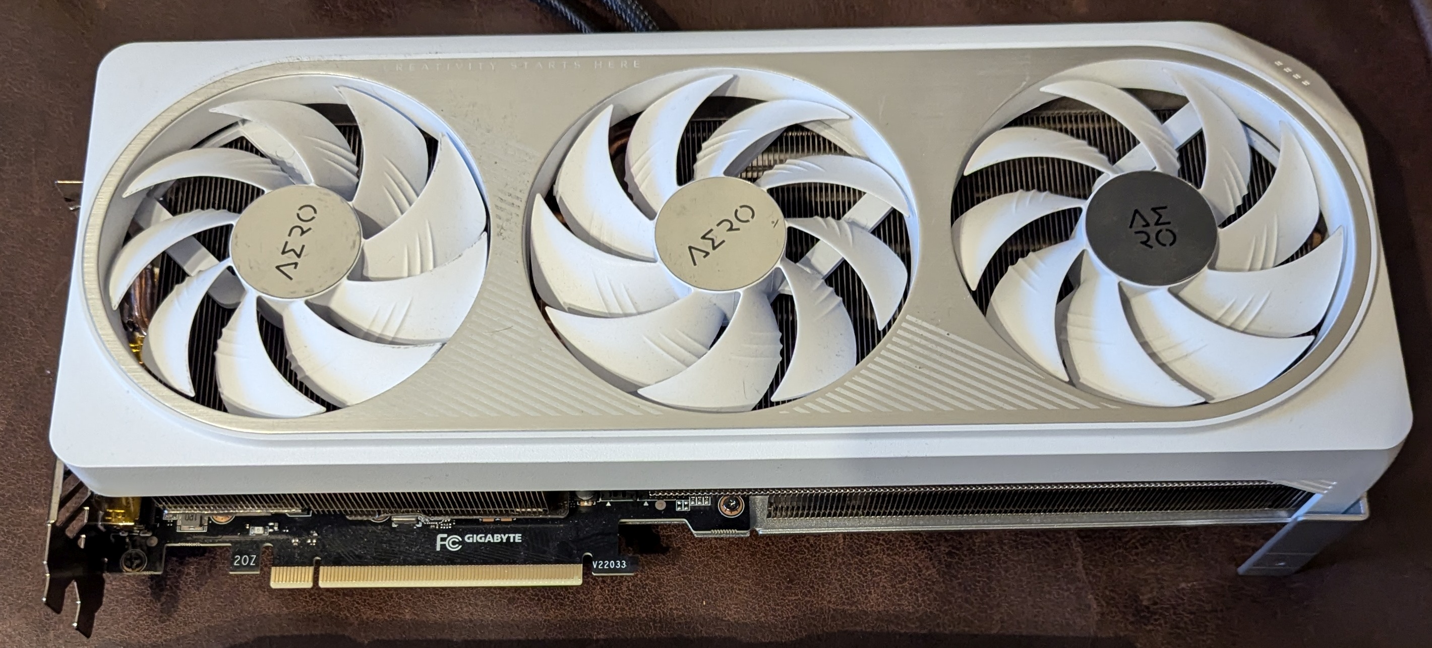 |
Gigabyte GeForce RTX 4070 Ti AERO OC 12GB - 2023
In the early to mid 2020s, video cards had massive cooler expansions. This 285 watt card was an enormous triple-slot flow through design! It was sent in by a friend, who was acting on behalf of someone else, he said it was out of warranty and faulty, but marginally so. With my characteristic avarice, a little curiosity, and wanton disregard for what free time I have left these days, I agreed to see what was wrong with it. Initial stability testing went well. Heavy GPU workloads like CUDA, OpenCL, etc. crunching always passed, but games never did. Unigine Superposition passed almost every time, Horizon Zero Dawn crashed around a third of runs, Cyberpunk 2077 completed about half of all benchmark runs. In retrospect, this made perfect sense, but I did not have that benefit then. I clocked the GPU up and down, loaded it up and down, these days a lightly loaded GPU can clock a lot higher than it can when it's heavily loaded (so power limited) and possibly exit the region it's stable within. The behaviour did not change. There were no display issues, no graphical glitches or corruption, so I tested the PCIe interface, dropping it from Gen 4 to Gen 3, I tried various board power limits. I did ten minutes OCCT VRAM test, which offered nothing, and I was really stumped. An inspection of the PCB revealed a potentially missing capacitor (later found to be not originally fitted) which was a lead for a while. I left it running the OCCT VRAM test, not expecting to find much (VRAM usually always causes display corruption)... to return to around 1.6 million errors. This wasn't entirely reproducible, the next test with the same settings resulted in 1,012 errors through the entire run (a working video card has zero), and a -500 MT/s clock offset on it resulted in a full pass. That was enough to diagnose it as a VRAM issue - Probably not a data issue, but a control one, maybe a RAS or CAS strobe was iffy, or a PCB trace was not quite there on the eye diagram. Anything can cause these, we have to limit ourselves to testing what we can measure. I then became curious as to whether VRAM could be overheating. Memory temperatures are reported as a "junction" temperature, an emulation or guess of what the temperature is on the surface of the package where the heatsink contacts. No sensor can be there, of course, and the RTX 4070 Ti's cut-back 192 bit memory bus is satisfied by six chips. A manufacturing defect in a thermal pad or any one of the numerous steps in giving just one number to gues the temperature of six individual chips, scattered across the PCB, could result in temperature looking low but actually being very high. So, I asked how old it was. More than three years or so and thermal pads can lose their effectiveness somewhat. The answer was that it was about two years old... This gave me pause. Gigabyte's warranty for a video card was (and is) three years. On checking the serial number, we had 11 months warranty left. An RMA was initiated and I ceased all other work on it. Gigabyte's RMA process is utterly bizarre. You have to fill in a form (actually an Excel spreadsheet) with fields highlighted for you to use, but not actually presented as a form. Then you have to ship it to Gigabyte's repair facility at your expense (by enclosing CASH in the box to cover return, is one option!). Gigabyte said they could not reproduce the issue, but offered to swap it for the Aero V2 model (slightly smaller cooler), which I accepted on Friday 11th April. On Monday 14th, Gigabyte sent a quite confusing email back now showing the fault was "O11 OS HANG UP" and they'd sent out the replacement, also showing the new serial number (a 0 changes to a 1 when you RMA, but the serial stays the same) and the same product code, GV-N407TAERO OC-12GD, as the one I'd sent back. The V2 had a slightly different code. The replacement arrived while I was out of town and, on returning, there was a completely good GV-N407TSAERO OC-16GD. One may notice this is a very different code: It was the RTX 4070 Ti Super 16 GB! Okay Gigabyte, you did right by me. I will buy more of your things. Without a working example of a 4070 Ti to examine, what we'll do here is have a quick look at what Nvidia initially did with the RTX 4070 Ti. The "Ti" models were historically a mid-life refresh where Nvidia felt it was necessary, though there were some exceptions - the GTX 660 Ti ($299) launched a month before the GTX 660 ($229), for example, but was quite limited in availability until well into 2013, after the Radeon HD 7870 proved to be problematic for the GTX 660. Nvidia releases variants of names, often with completely different GPUs under the hood. The GTX 660 Ti (which had a completely crazy memory layout) used the GK104 and the GTX 660 used the GK106, for example. One of the things Nvidia did which was highly unpopular was reducing the memory capacity but also reducing the GPU and sometimes memory performance at the same time, without making it clear. The GTX 1060 6 GB, for example, had 1280 shading units, but the GTX 1060 3 GB had only 1152. This was also the intention with the 4070 Ti. Nvidia announced the RTX 4080 16 GB would have 76 enabled SMs (so 9728 shader units) on its AD103 GPU and a 12 GB model would have a different GPU, the AD104, with 60 enabled SMs. It would have been substantially slower. It wasn't just mildly cut back, it was massively cut back and not even the same GPU! Then Nvidia, in its own words, "unlaunched" the RTX 4080 12 GB and renamed it "RTX 4070 Ti". Nvidia ultimately did the right thing there, but only after trying everything else. In the 4000-series stack, "model number inflation" had struck hard. The RTX 4070 occupied the place the "6" model had in previous generations and the 4060 occupied the "5" place, though it could be argued the 4060 Ti was the "5" and the 4060 was a "4" or "3"... Time for a table! We're not normally going to include "variants" like Tis or Supers, just focusing on the shitshow that Nvidia's numbering is. The Hattix 4000-Series Model Number Equivalencifinicator
Core: 80 ROPs, 240 TMUs, 2640 MHz RAM: 192 bit GDDR6X, 1315 MHz, 504,200 MB/s Shader: 60 SMs, 7680 individual shaders, 240 tensor cores, 60 RT resolvers MADD GFLOPS: 40,550 |
||||||||||||||||||||||||||||||||||||||||||||||||||||||||||||||||||||||||||||||||||||||||||||||||||||||
 [The AERO OC 4070 Ti Super uses the same cooler as the AERO OC 4070 Ti above, so here's the back instead] |
Gigabyte GeForce RTX 4070 Ti SUPER AERO OC 16GB - 2024 This was an RMA replacement for a faulty RTX 4070 Ti of the same Aero line, sent as "refurbished" and obviously used with very minor wear marks on it. That's expected, nothing bad. Nvidia had a rough launch with the 4000 series. The 4090 was very powerful, but in short supply and extremely expensive. The 4080 was equally as bad value as the 4090, which endeared nobody - Paying top price to be king was okay, but paying top price to be second best was not. At the other end, 4060 was a joke which forgot to be funny, while the 4060 Ti was funny and didn't realise it was a joke. Nvidia's entire line was being carried by the 4070 and 4070 Ti. So, just like when the launch of Turing (2000 series) was a disaster, Nvidia had a re-launch waiting. Even before the first 4000 hit the streets, everyone knew the "SUPER" refresh was waiting. This became even more obvious when we saw the launch day specs of the RTX 4080 16 GB (76 SMs, 716 GB/s VRAM) and RTX 4080 12 GB (60 SMs, 537 GB/s VRAM). There was enough room there to park another model in! As fate had it, the backlash on the RTX 4080 12 GB was so intense that Nvidia rebranded it, even before launch, as RTX 4070 Ti... Then, a year later, parked this 4070 Ti SUPER in the gap! 66 SMs, 672 GB/s VRAM, so a GPU a little above the RTX 4070 Ti, but not by much, and the VRAM subsystem from a 4080, declocked slightly. This is what the 4080 should have been on launch, and the 4080 itself should have been a 4080 Ti. TDP was 285 watts, same as the RTX 4070 Ti, and this is implemented as a "power limit" by Nvidia's BIOS. When 285 watts is hit, the GPU will throttle back. The single most important thing to get more performance out of a modern Nvidia GPU is not to overclock it, but to put the power limit up as high as possible. Undervolting can also help use less power, yet may also limit maximum attainable clock. It was usually about 10% faster than the 4070 Ti (which remained in production) and maybe 15% slower than the 4080. In performance, it went up against the RX 7900XT, which it beat when heavy raytracing was in use, but lost (by quite a lot) when it wasn't. It was what the 4070 Ti should have been on release day, but this wasn't possible... You see, gentle reader, Nvidia made only five Ada architecture GPUs. SMs in Ada were similar to Ampere, each GPC had six TPCs, each of which had two SMs, so a GPC had 12 SMs in it. The number of TPCs in a GPC could and often did vary. AD107 - 24 SMs, 32 MB L2 cache, 128 bit memory AD106 - 36 SMs, 32 MB L2 cache, 128 bit memory AD104 - 60 SMs, 48 MB L2 cache, 256 bit memory AD103 - 80 SMs, 64 MB L2 cache, 256 bit memory AD102 - 144 SMs, 96 MB L2 cache, 384 bit memory The attentive reader would see the original 4070 Ti, or 4080 12 GB, was set to 60 SMs so it could use the much cheaper AD104 GPU instead of needing cut-down AD103s. When the 4070 Ti Super was released, it could not use AD104, so instead used AD103 with 7 TPCs (14 SMs) disabled, probably one in each GPC, though AD103's last GPC had only four TPCs, not six. AD104 was similar, its last GPC had only five TPCs. Nvidia spent the year of 2023 stockpiling partly defective GPUs to power the launch of the "Super" refresh. AD103, the GPU in use here, was used in (consumer cards only), the RTX 4070 (AD103 variant), RTX 4070 Ti Super, RTX 4080, RTX 4090 Mobile Max-Q, and RTX 4090 Mobile were AD103-based. In this 4070 Ti Super, Unigine Superposition knocked out a 13,600 score (1080p Extreme) and Horizon Zero Dawn (Ultimate, 1440p) knocked out a 168 FPS average. 3DMark Steel Nomad bashed out a 5,780 score. To test it when it arrived, I did a benchmark pass of Cyberpunk 2077 in RTX Overdrive mode (57 FPS average at 1440p), then did the same with its power limit raised from 285 watts (stock) to 320 watts (BIOS maximum) and Cyberpunk 2077 came in at 65.73 FPS in the same preset at 1440p. Core: 96 ROPs, 264 TMUs, 2640 MHz RAM: 256 bit GDDR6X, 1313 MHz, 672,256 MB/s Shader: 66 SMs, 8448 individual shaders, 264 tensor cores, 66 RT resolvers MADD GFLOPS: 44,900 And we got to the end of a 4000-series entry without even shitting on the 4060 more than once! |
||||||||||||||||||||||||||||||||||||||||||||||||||||||||||||||||||||||||||||||||||||||||||||||||||||||
|
What is a video card? Theoretical and historical terms, computer video is an evolving proof of the Wheel of Reincarnation (see Sound Cards too) wherein: 1. A new type of accelerator is developed, which is faster and more efficient than the CPU alone 2. They eventually take on so much processing power that they are at least as complex as the host CPU 3. Functions done on the GPU are essentially done in software, as the GPU is so flexible 4. The main CPU becomes faster by taking in the functions that dedicated hardware used to do 5. A new type of accelerator is developed, which is faster and more efficient than the CPU alone Modern video cards are at stage 4, Ivy Bridge and AMD's Llano APUs represented the first generation of CPUs designed to be competent at demanding GPU tasks. They cannot match a GPU's memory bandwidth, so future accelerators will be about reducing this need or supplying it, but the GPU shader core is inexorably bound for the CPU die. Most CPUs today have hardware to decode and encode video as well as perform accelerated GPGPU compute tasks. The Current Cycle In the early days, the video hardware was a framebuffer and a RAMDAC. A video frame was placed in the buffer and, sixty (or so) times a second, the RAMDAC would sequentially read the bitmap in the framebuffer and output it as an analog VGA signal. The RAMDAC itself was an evolution of the three-channel DAC which, in turn, replaced direct CPU control (e.g. the BBC/Acorn Micro's direct CPU driven digital video) and even by the time of the 80286, the dedicated framebuffer was a relatively new concept (introduced with EGA). This would remain the layout of the video card (standardised by VESA) until quite late in VGA's life (early to middle 486 era) where it incorporated a device known as a blitter, something which could move blocks of memory around very quickly, ideal for scrolling a screen or moving a window with minimal CPU intervention. At this stage the RAMDAC was usually still external (the Tseng ET4000 on the first video page is an example) with the accelerator functions in a discrete video processor. The next development, after more "2D" GDI functions were added was the addition of more video memory (4MB is enough for even very high resolutions) and a texture mapping unit (TMU). Early generations, such as the S3 ViRGE on this page, were rather simple and didn't really offer much beyond what software rendering was already doing. These eventually culminated in the TNT2, Voodoo3 and Rage 128 processors. While increasing texture mapping power was important, the newly released Geforce and Radeon parts were concentrating on early versions of what the engineers called 'shaders', small ALUs or register combiners able to programmatically modify specific values during drawing, these were used to offload driver API code which set up triangles and rotated them to fit the viewing angle, and then another part where lighting was applied. These became known as "Transformation and Lighting" engines (T&L) and contained many simple ALUs for lighting (which was only 8 bit pixel colour values) and several, not as many, more complex ALUs for vertex positions, which could be 16 bits, but usually went as FP32 values. As it became obvious that GPUs had extreme levels of performance available to them (a simple Geforce 256 could do five billion floating point operations per second!), it was natural to try to expose this raw power to programmers. The lighting part of the engine became a pixel shader, the vertex part, a vertex shader. Eventually they became standardised into Shader Models. SM2.0 and above have described a Turing Complete architecture (i.e. able to perform any computation) while SM4.0 arguably describes a parallel array of tiny CPUs. SM4.0+ (DX10/11/12) shaders were very, very fast at performing small, simple operations repetitively on small amounts of data, perfect for processing vertex or pixel data. However, SIMD and multi-core CPUs are also becoming fast at performing these operations and much more flexible. This has led many to believe that the lifespan of the GPU is nearing an end. By saving the expense of a video card and using the extra budget to tie much faster memory to a CPU and add more cores to the CPU, a more powerful machine even when not playing games could be likely realised in future PCs. A modern GPU's array of shader power is the extreme of one end of a scale which goes both ways. The far other end is a CPU, which has few but complex cores. A CPU is much faster on mixed, general instructions than a GPU is, a GPU is much faster on small repetitive workloads. The two extremes are converging, CPUs are evolving simpler cores while GPUs are evolving more complex ones. A noteworthy attempt was Intel's Larrabee design, ultimately becoming Xeon Phi, a "manycore" CPU, intended for highly threaded workloads. Larraboo was actually an array of 16-48 modified Pentium-MMX cores which run x86 instructions, truly emulating a hardware GPU, Larrabee has no specific video hardware and could, with some modifications, be used as a CPU, though it would be incredibly slow for the poorly threaded workloads most CPUs handle. Larrabee was too much, too soon, and went nowhere. Why do CPUs and GPUs differ so much? Why haven't they merged? Why does Intel spend so much die area on an IGP on practically all of its consumer products? In many cases, it's more than half of the CPU being burned on a GPU which might never even be used. As of 2024, Raptor Lake S was actually a weird oddball, the XE-LP graphics engine was very small on the die (and incredibly low performance), as Intel wanted to fit in eight big Raptor Cove CPU cores and four Gracemont ("Atom") clusters, so 16 Gracemont cores, as "E-cores". The E-cores took the die area ther GPU would have traditionally used. CPUs are latency machines. They do everything in their power to reduce latency. Sticking with the Raptor Lake example, it has 36 MB level 3 cache, then 2 MB L2 cache dedicated to each Raptor Cove core (and 4 MB L2 cache for each cluster of four Gracemonts). If you want some data or an instruction, the CPU is designed to make sure that the chances of it being in cache are as high as possible. Each CPU can run another thread if one gets stalled waiting for memory, that penalty is very high. L1 cache has your data in around 1.5 nanoseconds. L2 cache responds in around 4 ns. L3 cache, around 80-100 ns (and purely exists to save power on going off-die to DRAM). System DRAM, the highest performance RAM money can buy, around 80 ns. We probably shouldn't even include SSDs here, but a very fast PCIe 5.0 SSD will respond in around 50,000 ns. AMD does caching differently, its L3 cache is twice as nimble as Intel's so actually improves performance: Best seen in AMD's X3D CPUs and their dominant performance. So, ideally, we want data in L1 or L2 cache, but that's small and it's very hard to make it large while keeping it fast enough. Intel goes with a large and slow L2 cache, AMD with a smaller but faster one, as it has L3 to catch it if it misses. There are tradeoffs here, we can use the same die area to have an extremely large L3 cache with a smaller L2 cache, or a very large L2 cache and a smaller L3 cache, but a larger cache is necessarily a slower cache. GPUs are not latency machines. Latency doesn't really matter much to a GPU. While a CPU has a few dozen threads it can handle, GPUs work on thousands at once. If one thread is waiting for data from memory, there are scores more waiting to run. GPUs are bandwidth machines. Compare a freight airplane to a bulk carrier ship. The plane can get you 50 tons of cargo in four hours. The bulk carrier can get you 100,000 to 400,000 tons of cargo, but in days. There's also the container ship, which is around twice as fast as a bulk carrier and can contain around one tenth of the weight of useful payload: Most containers weigh more than their contents! In this analogy, the cargo plane is a CPU's L1 and L2 caches. The bulk carrier is RAM. The container ship is an L3 cache. Now we have 500 work sites which all need 200 tons of material (100,000 tons total). Do we just load it into 2,000 cargo planes? It'll get here in four hours! Well... We don't want that. It's way too expensive (and the world doesn't have 2,000 50 ton cargo planes we could charter at short notice). Each site doesn't need all 200 tons at any one time, it has nowhere to store it all, so there's no need to rush it, and they're going to be delivered 10 tons at a time by road vehicles anyway. While any one site is working on what it's doing right now, it can be using the employees while another site waits for material to arrive. When the first site is done, the employees can move to the next site which has the material. We can employ as many workers as we need, so long as the material arrives when it's needed. The important thing is that it doesn't actually matter how long the material takes to get here. We can order it way in advance. That's how a GPU works. It doesn't care how long data takes to arrive after being requested, only that an awful lot of it is arriving at any one time. Any individual thread can wait, it has far more threads than the ability to process them all at once. |
|||||||||||||||||||||||||||||||||||||||||||||||||||||||||||||||||||||||||||||||||||||||||||||||||||||||
|
The Rule of Alternate Generations A very reliable way to tell if a GPU generation will be any good will be to ask if the previous one was bad. A quick list will help. The "?" column is "Should you buy this generation from this manufacturer?"
AMD has 7 alternations, so "Was the previous generation not X" is not a good way to solve for "X" on AMD. Nvidia, however, has 13 alternations. "Was the previous generation not X?" is a very accurate way to solve for "X". So, if the previous generation was "not good", the next Nvidia generation probably will be good. Likewise, if the previous generaiton was "not bad", the next generation probably will be bad. "WAIT!" you cry "You're including some fake AMD generations!" and you'd be right - we didn't include Geforce 100, 200, or 800, which were all fake generations, and GeForce 600 and 700 were the same generation too! Let's run that AMD list with just generations where there is something actually new instead of just minor process improvements (not new nodes) or renamed SKUs.
Why does this happen, and why's it mostly Nvidia? It's mostly down to how R&D works. Nvidia wants a rapid release cadence, (it's down to around 24 months now, but was annually early on) but GPU design and GPU supporting software development is slow. Nvidia can't ground-up redesign everything. For example, the basic shader architecture of Maxwell was evolved into Pascal, Turing, Ampere, and Ada. Maxwell itself was a big step from Kepler, but Kepler still provided the basic stepping stones for Maxwell. AMD, on its side, evolved Khan (R300) into the R400 and R500 as ATI, then evolved R600 into Terascale, then Terascale 2, then Terascale 3, then a more or less ground-up redesign into GCN, which was extensively evolved through to Vega, its fifth generation. AMD, as of 2025, was four generations into RDNA, although Navi 3 was very, very similar to Navi 2 and Navi 4 was a huge uplift. This is the major reason why we see alternating generations. If a previous generation didn't do well, then the next can be rapidly re-synthesised to optimise it for whatever went wrong. For example, AMD Polaris (RX 400) did very badly, as it couldn't compete at the high end. So, AMD optimised for low cost with a Polaris refresh. They stuck on the 16FF process at TSMC and used improvements to that process to gain a higher yield and run either lower powers or higher performance, so the Radeon RX 500 generation was cheaper and faster than the 400 generation. There's also that a poor "tiny refresh" generation gives the designers time to finish a big architectural change. AMD's RX 500 was giving AMD time to finish the Navi (later "RDNA") architecture. Other times, we want to introduce distinguishing features. Nvidia devoted a lot of Turing's die area to RT solvers and tensor cores, but kept most of the same Pascal CUDA capability and rasterisation performance. This meant Turing had big, costly dies, (Pascal + RTX meant the RTX hardware had to be added on, taking space and raising cost) and didn't outperform the previous Pascal generation very much. On some SKUs, Turing was a step back: RTX 2060 was the same price as GTX 1070, but significantly slower. RTX 2080 had a similar sized die to GTX 1080 Ti and Titan Xp, and a similar feature count (13.6 billion vs. 12 billion) but was not much faster. Turing had made improvements to the basic Pascal architecture, but minor ones and, ultimately, the addition of extra special function hardware meant Turing had less compute resource available to it. TU104 and GP102 were similar in size and feature count, but TU104 only had 3072 CUDA cores, while GP102 had 3840. TU104 could clock higher and therefore use more power to help narrow the gap, and still only emerged very slightly ahead at a much higher cost. These are two examples and there are many more. Maxwell (GeForce 900) to Pascal (GeForce 1000) should have been another bad generational shift, but Pascal came with both the revised architecture, availability of very fast GDDR5X memory, and the new 16FF process at TSMC. This was all very risky, but the risk paid off. Maxwell had originally been designed for TSMC's 20nm process (which became 16FF) but TSMC limited that process only to mobile and low power, so Qualcomm and Apple ate it all and Maxwell was resynthesised for TSMC's then-highly mature 28HPM process. Maxwell's own architectural advancements (mostly its huge L2 cache!) saved the generation from being a disappointment (it was just over a year late) but also the design having initially been intended for 20nm helped it become Pascal on the closely-related 16FF process more easily. At the same time, AMD was hedging its bets. Polaris was just a re-synthesis of the previous Tonga (GCN3) from 28HPM to 16FF. AMD was unwilling to change both architecture and process in the same generation (this is a major driver of the Rule of Alternating Generations) and, while Polaris was indeed lower power and clocked higher than Tonga while still having more hardware on die, it was the same basic architecture. |
|||||||||||||||||||||||||||||||||||||||||||||||||||||||||||||||||||||||||||||||||||||||||||||||||||||||
 Hattix hardware images are licensed under a Creative Commons Attribution 2.0 UK: England & Wales License except where otherwise stated.