
|
DTK PEM 2500 This is typically what you'd see in an early 386. Notice at the top left of the board, no fewer than three crystal oscillators. Just right of the 386 CPU is a full 64kB of SRAM cache - this would have been an amazingly fast 386 board. Most boards either did not have cache or had unfilled sockets for it. 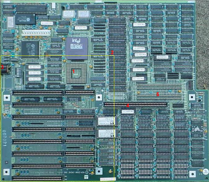 Back then, boards weren't obsolete in ten minutes and most chips were socketed to facilitate replacement, since motherboards were so expensive that labour costs paled into insignificance. This perhaps explains why this board was supported up until at least 1990 (the BIOS date, but that's not the original shipping BIOS) and long after 256kB cache boards using more integrated chipsets had appeared.
Note that there's no chipset, just bundles and bundles of logic. The only thing approaching a chipset is the VLSI chip which is probably an interrupt controller just left of the CPU. This 32 bit motherboard would have been paired with a stronger 386, perhaps a 25 or 33 MHz one. The 386SX boards were really souped-up 286 boards, and just as 16 bit as all 286s. This severely harmed their performance due to half the bandwidth... and who puts expensive cache on a low end board? The image is from an older site I used to have, so it's annotated with... Points of Interest 1. This is a 387 FPU socket. 2. 10 SRAMs to make 64kB of cache. These are 64kb chips with two extra for parity. This can be reconfigured to 256 kB. 3. AT keyboard connector...just look at the placement! 4. Slot for a propreitary memory card. 5. SIPP RAM holes. Yellow box - The size of a Baby-AT (the 'full size' things from the early Pentium and 486 era!) motherboard in comparison. On the note of comparison, check out the sheer component count! This is partly why IBM said 386s were too expensive, their supporting motherboards were astronomically complex. A 386 powered PC in the early 1990s or late 1980s was beyond the budget of mortal men. Corrected for inflation, a well loaded 386 at 33 MHz with 4 MB or 8 MB RAM, a 40-80 MB hard drive and a 256 kB VGA card, a high end desktop would be, and this is in words, ten thousand American dollars. CPU support: 386DX Best with: 386DX-25 |
|||||||||||||||||||||
|
MG 82C480 In 1993 there was a fire at a factory supplying DRAM and SRAMs. As a result, cache RAM became socketed and boards could be ordered without it fitted, because it was very expensive. It wasn't even for upgradablility, the sockets could only take one type of SRAM! This is a board from that era, but one sold to the very bottom of the barrel. 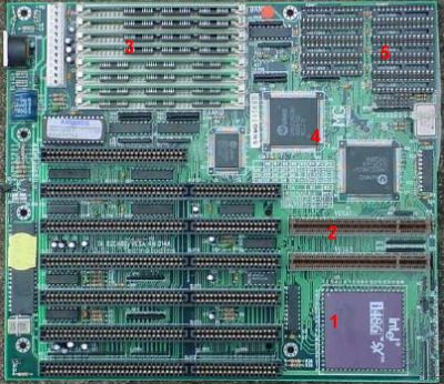 The board itself is very good and highly regarded, but this one shipped with no cache and in one of the "sucker configurations" of the mid-1990s. Anyone in the know would have used the money spent on this on an AMD 386DX40, mounted on a motherboard with 64 kB (or more) cache, and a decently fast hard drive. 486SX-25 was the slowest 486 made, the FPU disabled (nobody cared), but, of course, ran on that very slow 25 MHz system bus. Even with 486's onboard 8 kB L1 cache, a motherboard with no cache and the 25 MHz memory access enabled a 386DX40 to keep up: For around 75% of the price.
 Removing the CPU's L2 cache was an enormous downgrade, the CPU would then be perhaps 40% of the performance it would be with cache. Practically all 486SX-25s were perfectly happy running at 33 MHz and would see a significant uplift from it, as everything else also then ran 7 MHz faster! This meant there was a cottage industry in Asia exploiting the USD$ 50 difference between the 486SX-25 and SX-33. They'd buy up the SX-25, erase the markings, and replace them with markings copied from a 33 MHz. They'd then sell them on at a profit. This was known as "re-marking" and would become a significant problem by the Pentium-MMX. This one could be upgraded to a DX50 or DX75 (it was intended for a DX50) but was fixed to a 25MHz system clock. Points of Interest 1. One of the worst CPUs ever, the 486 SX25. 2. VESA Local Bus slots. This board layout was nearly canonical at that time to accomodate VLB. 3. Eight 30-pin SIMM slots for a maximum of 8MB RAM. 4. UMC 481 chipset. Highly regarded. 5. Nine empty SRAM sockets! Eight plus parity, about $30 USD (this would have been $60 or more at the height of the crisis) of cache chips is quite a saving when you're making a really crap PC. Boards could be ordered without cache, but it was very silly to do so. CPU support: 486 Best with: Cache SRAM! |
|||||||||||||||||||||
QDI 895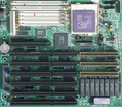 By 1995, Intel's Pentium still hadn't caught on despite being introduced in 1993. Intel had a lot of problems producing it and just couldn't get the price down. Indeed, 1993 was the year of the 386DX40. This is what you'd see in most 486s sold by shops intent on keeping a good name for themselves if they weren't a UMC-only house, which were quite common. (The rest would be doing PC Chips...)
The OPTi 895 chipset was a nightmare to work with, coming in many different version each of which had their own style of jumper setting. Note the long DIP chip just left of the main bank of ISA slots. That's the AMIKEY keyboard controller - nothing more than a licensed 80C42 microcontroller, as seen in boards ever since the 286. You can see one in both previous boards. (Very top left on the DFE, same position as here on the MG.) When PCI took over and brought the LPC bus to handle standard I/O and ISA, the seperate keyboard controller would be annexed into the southbridge. We were now down to the Baby-AT form factor which would survive as standard until ATX took over. The OPTi chipset was one of the early "Northbridge" and "Southbridge" combinations. The northbridge, the larger chip, handled RAM and fast I/O, like the three VESA Local Bus slots. The smaller rectangular chip was the southbridge (this would become just the "Super I/O controller" a few years later) and handled I/O, so all the rear ports and the keyboard. This board is also notable in that it has eight cache SRAMs by the bottom right. This means the cache was not ECC or parity protected. Points of Interest 1. AMD 486DX100. If you weren't a big OEM, you'd be using far more Cyrix and AMD chips than Intel. They worked just as well (or better) and were a lot cheaper. 2. OPTi 895 (revision 3) chipset. OPTi would later lose a lot of influence and eventually leave the business with a hell of a broken (and highly anticipated) Pentium chipset. 3. 30 pin SIMMs were still popular in banks of two. Two 16bit SIMMs would satisfy the 32bit bus of a 486. 4. 72 pin SIMMs had been released by this time - a single SIMM could match a 486 if you used 72 pin, but many liked to re-use their older 30 pin and add wait states to match the faster bus. That'd have been a performance killer in a system as fast as this, which was really wanting at least 70ns FPM RAM and preferably 60ns EDO. CPU support: 486 Best with: 72 pin SIMMs and a 486DX/4 | |||||||||||||||||||||
|
Soyo SY-25P Submitter Lee Caskey writes: 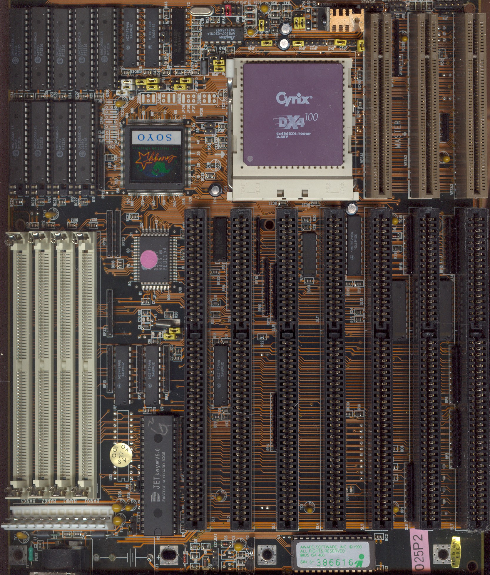 "This was salvaged during my college years and used as a testing and programming platform while I was system administrator of my college. It was also fun to play old-school games on. It actually ran Win95B rather well when loaded with 64Mb of EDO RAM, the onboard 256Mb cache chips didn’t hurt either. It ran the gamut of 486-era processors from a TurboChip 133, to a AMD DX4-100 and even a Intel DX2 66 before I finally settled on the Cyrix chip. It’s lack of a hardware IDE drive interface required a VESA bus controller card. Also it required an external battery to maintain its BIOS settings, fortunately these seem to last forever."
This board is right at the time when building PCs stopped being exclusively between large companies and bearded techs in a darkened room and the parts started becoming available in retail channels. The time was also a transitional one in many other ways. The bandwidth limits of EISA had long been feared and were being reached, but there was no consistent solution. The brown ports you see here are VESA Local Bus ports where peripherals were actually added to the CPU's local bus, the FSB. Rising FSB speeds and uncertain FSB clocks made VLB a chancy proposition and there was little support beyond certain high end video cards. When Pentium arrived with 50, 60 and 66MHz FSB clocks, VLB was abandoned entirely, its successor was PCI. Visible on the top left is another legacy of older motherboards, onboard cache. Level 1 cache is sometimes called "internal cache" and level 2 "external" because L2 cache indeed was external. This particular cache consists of UM61256AK-15 CMOS SRAM in a 28 pin DIP3 package with organisation 32K x8, giving each chip a capacity of 256 kilobits. With eight of them, the bus becomes 64 bits wide and 256KB large, but the bus is actually only 32 bits wide and the SRAMs are organised in two banks of 32 bits. A single lone chip at the top right of the cluster is the parity buffer, as evidenced by the two 74xxx series 8-bit CMOS buffers right next to it. At the bottom left is another sad legacy of PC history. Back before time, before the Big Bang, before even IBM, keyboards were just serial devices and they had their own microcontroller onboard to give them their 'smarts' and send the correct byte code when a key was pressed. This keyboard controller was moved internally very early in the PC's history and became the "Keyboard BIOS", though it was not truthfully a BIOS. Near that is the real BIOS, an Award system which would still be familiar today, BIOS UI having all but ended its evolution even this far back. AMI had introduced an utterly horrendous mouse-driven BIOS interface not long before and as a result, board makers stopped using the once-dominant AMI BIOS. A GUI BIOS is not necessarily a bad thing but AMI's attempt certainly was and this cast a long shadow over any future attempts of GUI BIOS The system chipset is under the Soyo Energy Star sticker, it was very common back then to put a sticker on the main chipset (the bus controller, the Northbridge) and the Southbridge, the I/O controller, was just starting to emerge as one chip. It can be seen just below the main bus controller with the pink sticker on it. It seems Soyo didn't want people to know the chipset in use! The chipset in use was an SiS. Back then, of course, the actual chipset didn't much matter. System architecture was quite simple, you had a host chip which the FSB originated from, going to the CPU. This also handled L2 cache and tag RAM. From that you had a memory controller, the "southbridge" on this motherboard which sat on the CPU's address bus. The data bus went through the "northbridge" to the CPU's FSB. The board layout, number of ISA slots, positioning of the chipset, CPU socket, cache, RAM, VESA slots was absolutely typical for an early 1990s 486 motherbard; Almost all of them had some variation on this basic layout. One of the first was the PX486P3 and, any manufacturer who didn't lay out his board like that had to reduce something. Maybe fewer RAM slots (like on this, only four, the standard was eight), maybe less cache, maybe fewer ISA slots...but regardless, he was almost certain to lose money. The layout of this particular board looks more like something out of the 386 age than mid-486, components absolutely everywhere. When you recall the standard VLB/486 board fashioned after the PX486P3 you realise what's going on with the Soyo board. It's tiny! Where are the hard disk connectors? The floppy header? Headers for serial and parallel ports? The SY-25P had none of that, instead relying on a port controller card which sat in an ISA port but also used the VESA ports. This card would provide the serial and parallel on the back or give headers for them. It'd have the IDE channels onboard and finally the floppy disk controller port. But why? Why would any manufacturer do that? Namely, the SiS chipset used likely did not support LBA addressing, so hard disks above 520MB would cause problems. An add in card was free to support whatever it liked. The alternate explanation is that the SY-25P was produced to order by Soyo for an OEM customer, such as Compaq or Gateway, who needed a specific configuration. So there you have it, a mid-486 era motherboard designed much more like the old early 386 motherboards which was certainly not a bad thing but not for the faint of heart. CPU support: 486 Best with: 486DX 80-100 MHz |
|||||||||||||||||||||
|
Gigabyte GA5-AX While boards from the likes of FIC using VIA's powerful MVP3 chipset were sometimes faster (especially with 1MB or 2MB of cache), they were never quite stable in some conifigurations due to issues with the SDRAM controller which VIA would finally correct in the KX-133 Athlon chipset. Find the right RAM, and they were solid, but the trick was finding the right RAM. That said, the Super-7 motherboard to buy, if you could afford it, was the FIC VA-503+  ALi's Aladdin V chipset was capable of doing what it claimed it could, doing it reliably and quickly, but it had one major flaw; AGP. While this board does have an AGP slot, few were willing to take the chance. Way back when I had the baby brother to this (the GA5-AA), an ATI Rage128 worked well with some issues, a Voodoo3 was perfectly happy, but a Voodoo Banshee didn't work at all.
Earlier versions of the Aladdin V had non-functional L2 tag RAM. This is the RAM which is used to organise and "tag" pages in L2 cache, which was external to the CPU and motherboard mounted. Gigabyte mounted distinct L2 tag RAM on the motherboard, the RAM chip is between the L2 cache (immediate left of ALi Northbridge) and a MOSFET just above the lithium battery. This had the effect that the cacheable area of L2 was 128 MB. Any RAM more than that, and the board did support RAM north of that, was outside the cacheable area. Revision H of the chipset fixed the problem, but Gigabyte never enabled internal L2 tag. A user-made BIOS enabled it by comparing it to the similar Asus P5A. Programs like WPCREDIT were able to adjust chipset settings on the fly, but L2 tag has to be done at boot, hence the need for a customised BIOS. Gigabyte had long been unable to write a manual, despite spending more and more paper on it with each new motherboard and this board sets bus, multiplier, and voltage settings with DIP switches. The manual included a table of CPUs and which settings to use for each one... but did not include how to set a 95 MHz bus, or a 4.5x multiplier, or a 2.2 voltage. You had to work that out yourself. Later revisions (and the GA5-AA smaller version) included a supplement with a full table of settings. You'd pair up a 100 MHz Super-7 motherboard with a K6-2. It was a canonical configuration. The K6-2 300 at first, a year later the 450 was the one to go for. This board has only 512 kB L2 cache, but boards with 1 MB were quite easy to get hold of, and really did make a difference. By this time, motherboard design had more or less standardised. Everything hung off the PCI bus, the Southbridge was a PCI device connected to the Northbridge by a PCI interface. It then did a PCI to PCI bridge to the system's main PCI slots and other onboard devices. The two ISA slots (one or two was still common) were again on a PCI bridge. So we had the core system based around the Northbridge, with the CPU, L2 cache and RAM hanging off the Northbridge, then a PCI bus going to the Southbridge, where everything else was connected. The original Southbridge use, to control external I/O, had been passed over to a WinBond or ITE "Super-IO" chip. This did the serial and parallel ports, JTAG, I2C and a few other things. Many of them could also handle an ISA bus. The Super-IO chip here is the "EliteMT" chip just left of the Northbridge. Below it is the L2 cache. In this era, system architecture was starting to change, as a result of the AGP bus. Older systems, like Intel's 430 series (e.g. the well regarded 430TX), had the Northbridge handling the FSB, RAM and PCI bus. The Southbridge was a PCI device itself, and sat as the last device on the PCI bus, bridging to ISA, providing the IDE slots, etc. Super Socket 7, or just Super 7, changed this somewhat. The Southbridge was now the only device on the Northbridge's PCI bus, and hosted all the PCI slot and onboard PCI devices PCI bus itself, so it became a PCI-PCI bridge. This can be clearly seen on the GA5-AX, the series of traces snaking from the Northbridge, under the RAM slots, behind the AGP and to the edge of the board beforre looping into the Southbridge is the interconnect PCI bus. All the other PCI slots, and the Super I/O chips (EliteMT used here) are sourced from the Southbridge. Not everyone did this chipset architecture. VIA, in particular, never bothered. The KT133 chipset (and subsequent VIAs before they moved to a custom chip interlink) had the 686A or 686B Southbridge hanging off the same PCI bus as all the slots. CPU support: Pentium, Pentium-MMX, K6, K6-2, K6-III, Cyrix 6x86/MII, IDT WinChip2 Best with: K6-2/400+ or K6-III 400+ |
|||||||||||||||||||||
MSI MS6156 Before MSI decided to start giving their boards names it was just MSxxxx and so it is with the MS6156, a completely unremarkable mini-ATX Slot1 motherboard often used by Fujitsu-Siemens. This one was absolutely bog-standard for the day. The rear had two serial ports under the parallel, three audio ports (line out, line in, mic in) under a game/MIDI port and two USB next to the PS/2 ports.
Sound wasn't bad, being provided by the Ensonique ES1373 (aka SoundBlaster PCI128) but otherwise the motherboard was exactly what you'd expect from something intended to be sold to and by OEMs. Minimal silkscreening (the white print on a board), no provision for a case fan and the cheaper VIA VT82C693A (Apollo Pro 133) chipset which had some reliability issues at times (very temperamental about RAM) but could run a 133MHz bus and 133MHz RAM. OEMs had to use the Apollo Pro 133 chipset because Intel was unable to provide a chipset able to run their 133 MHz CPUs (the PentiumIII-E)! The i820 chipset was a comedy of failings. Intel attempted to make a very large amount of money by replacing the industry organisation JEDEC (Joint Electronic Devices Council) with Rambus, Inc., a company Intel had significant share options in. So, Intel's i820 chipset, the only one supporting 133 MHz operation, only ran with RDRAM by Rambus, Inc. i820 was unstable with three RAM slots filled, so motherboard makers had to quickly seal off, tape off, whatever, the third slot. RDRAM was slower than SDRAM and a lot more expensive. It also could not be produced in quantity. Intel then made a "Memory Translator Hub" which would convert SDRAM signals to RDRAM ones for the i820. It was not stable and Intel had to recall 900,000 chipsets, but offered no financial compensation for the motherboards manufactured with them. Eventually, the RDRAM fiasco was to bite Intel again with the Pentium 4, but that was in the future for the Pentium III. Intel had scuppered any chance of the really very competitive Pentium III-E actually competing with AMD's Athlon and surrendered the high end to AMD. The SDRAM-supporting i815 chipset which Intel hurredly designed, halved the size of the in-order buffer from the legendary 440BX and so significantly underperformed it. This particular board was supplied with a PentiumIII 600E, the Slot-1 Coppermine with 256k on-die L2 cache but only a 100MHz FSB. Due to the larger capacity of a Slot-1 heatsink, that chip could almost certainly be clocked to 133MHz FSB and run at 800MHz which was more standard for Coppermines. CPU support: Celeron, Pentium II, Pentium III Best with: Pentium III 700 |
|||||||||||||||||||||
|
Abit BP6 Legendary. Truly, truly legendary. Very few motherboards had the kind of impact on enthusiast or high-end home computing that the Abit BP6 did. You see those images right: That's two Socket 370s.  Intel never made a BIOS or a specification to allow Socket 370, then for Celerons, to run SMP - But Intel did not disable the interface on the Celeron which allowed it to select being CPU 0 or CPU 1.
Additionally, the 440BX chipset also took no measures to limit dual CPU operation: It couldn't due to how the GTL+ FSB was implemented. A northbridge either had to support 2 CPUs or 0 CPUs, and the latter was just silly. 440BX itself was legendary also. Until VIA's Athlon-based KX-133 chipset, BX was the fastest memory controller anywhere. It could only officially run at 100 MHz, but had the facilities to clock the FSB and RAM to 133 MHz, but this took AGP to 88 MHz, well out of spec. BX had 1:1 and 2:3 AGP:FSB ratios, but 1:2/1:3/1:4 PCI:FSB ratios. Most video cards worked well enough on 88 MHz AGP. Abit stepped in, wrote the proper BIOS for it, laid the traces and the result was legendary. Two Celeron 300As at 450 MHz each were enough to stomp all over anything and everything. £400 would get you a high end dual-CPU workstation. Before the BP6, your SMP options were Pentium II Xeons or elderly Pentium Pros, where a single CPU alone would cost much more than an entire BP6 system. In about 2006, long after they were obsolete, I came across a pair of Pentium II Xeon 450/2MB CPUs, the highest end Xeon for some time. They were £2,100 each at the same time a BP6 was on the market. Later, Intel was to realise there was a market for SMP outside huge servers and officially sanction SMP on Slot-1 with the Pentium-III (a Shuttle HOT-649A I had was one of the best here). BP6 was first, though. CPU support: Celeron, Celeron-A Best with: Celeron 300A at 450, natch! |
|||||||||||||||||||||
Abit KT7 The KT7 was the first Socket A motherboard to be not crap. In the days of the first Thunderbirds and Spitfires (Athlon-B and Duron-A), the KT7 was the board to have. It ran paranormally stable, was capable of overclocking well beyond what you'd expect. In my use, it took a stick of memory rated for 66MHz to an incredible 152MHz.
The KT7 was incredibly popular among enthusiasts, as was its successor, the KT7-A. Primary among the reasons why was the VIA KT133 and KT133A chipsets, the highest performing SDRAM chipsets ever made on any platform. The blue and white wire you see in the image is a voltage mod, which adds 0.25V to the CPU core voltage. The RAID variants of this motherboard used the Highpoint 370 and 370A chips. Users of Windows Vista will find that the XP drivers for the HPT370 work just fine and in fact perform a little better under Vista, due to the streamlined disk access stack in Vista. The MOSFETS on this board show Abit's then-trademark overengineering. The CPU supply is three-phase and even the RAM has its own single phase supply. This overengineering was expensive and Abit's motherboards were not cheap. Not long later, Abit would run into financial difficulty and the engineers responsible for this glorious motherboard would go to work at DFI, transforming DFI from a middle of the road uninteresting vendor to the enthusiast's prime choice, just as Abit had been. This particular board powered the very first incarnation of this server. CPU support: Athlon, Duron Best with: Athlon 850-1000 |
|||||||||||||||||||||
FIC FA15T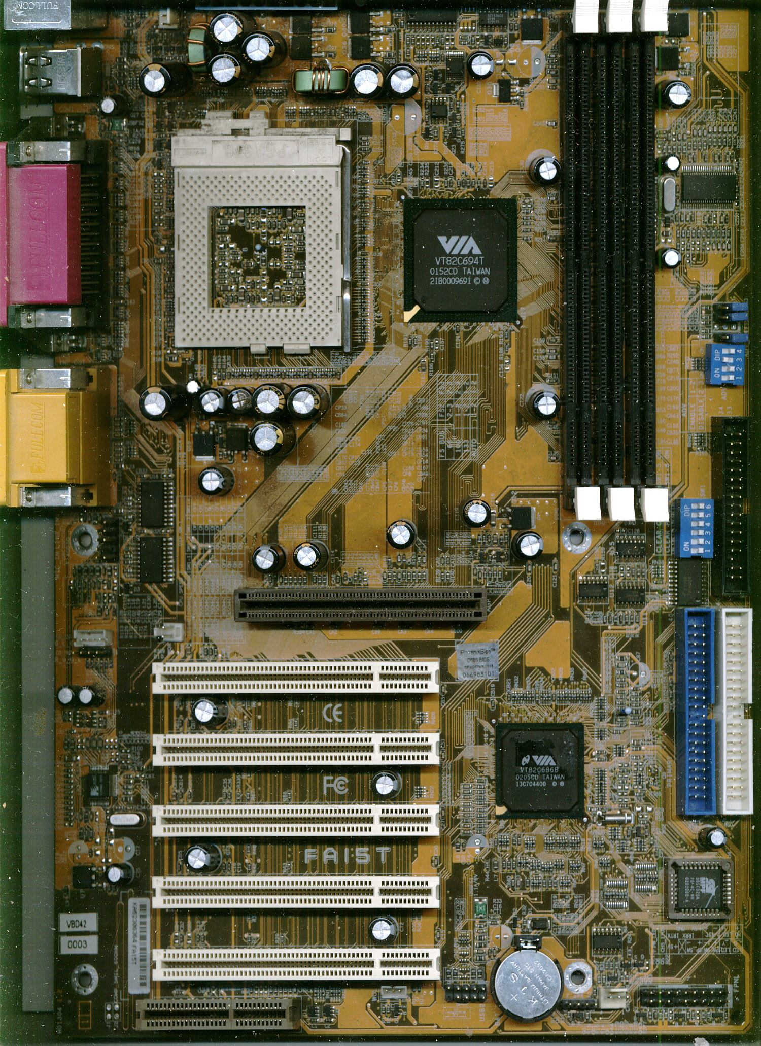 At this time, dated to late 2001 by the presence of the VIA 686B southbridge, VIA was a strange company. Nobody could beat their Athlon chipsets, KT133 was spanking even the mighty 440BX in SDRAM performance, but their Intel chipsets were usually that bit temperamental.
Many years later we learned this was because Intel published incomplete specifications, not incomplete enough to breach contractual obligations, but still falling short far enough to hinder intercompatibility. FIC, for their part, had always had a very close relationship with VIA and were usually first to market with a new VIA chipset. In this case, the Apollo Pro 133T, newly qualified for operation with the new Pentium-IIIS Tualatin-core parts. By the time we'd hit the Apollo Pro 133 chipset, VIA had ironed out all the edge cases of their Intel chipset and was actually offering the highest performance 133 MHz chipset on the market! Against the RDRAM-crippled i820, the VIA 133T easily won, but against the best Intel had, RDRAM i820 (slow) or cut-down SDRAM i815 (slower), Apollo Pro 133 was actually the fastest. VIA chipsets on Intel generally took more attention to get peak performance but once at peak performance they were certainly competitive. The FA15T was from the first (and only) generation of revised Tualatin-compatible boards, others included Asus' well regarded TUSL-2 and TUV4X (also using the 133T chipset) but all followed the standard layout seen here which was something of a de facto standard during the later SDRAM and early DDR days, RAM to the right of the CPU with one AGP and five PCI below the CPU with the southbridge just to the right of them. 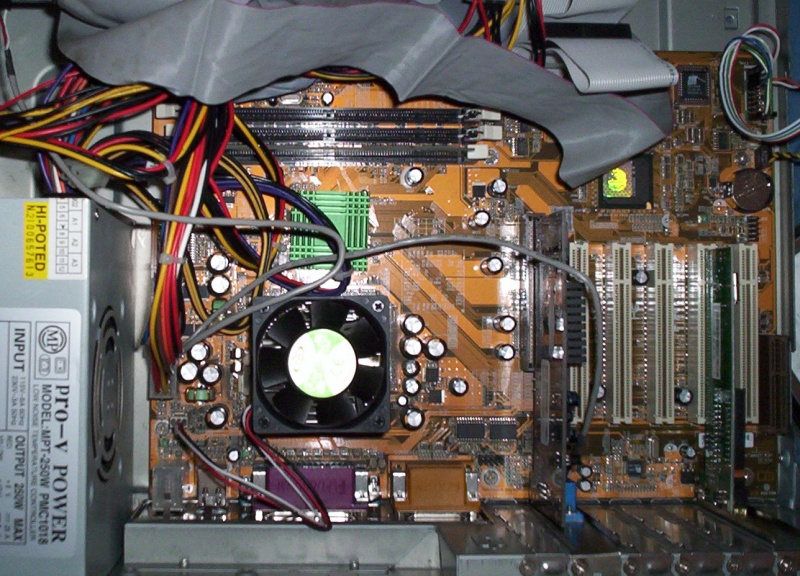 As configured, likely with either a 64 MB or 128 MB PC100 or PC133 SDRAM and, if I recall right, the video card was a TNT2 M64 This one was recycled from a nearby school, which had recently discarded a good number of them, and powered the server you're reading this page from until mid-March 2008, running a 1GHz Celeron underclocked to 750MHz. It was never really happy for whatever reason. I didn't have the inclination to find what the issue was, but at the time I suspected RAM. CPU support: Celeron, Pentium-III Best with: Pentium-IIIE around 800 |
|||||||||||||||||||||
EPoX KL133-ML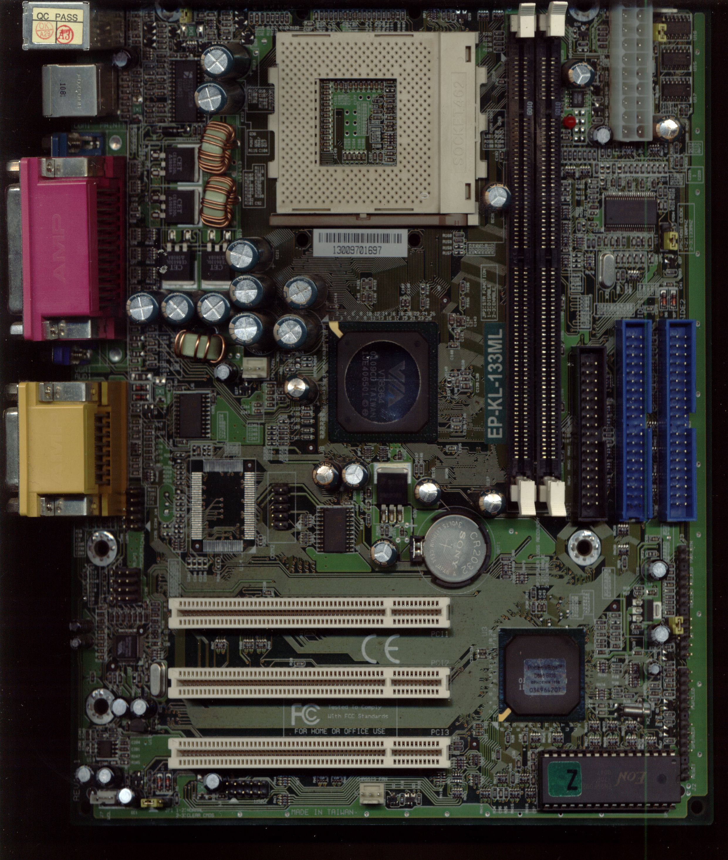 Micro-ATX with onboard-everything and based on VIA's highly integrated KL-133 chipset, which was the KT-133 with onboard S3 ProSavage video, a rather feeble 120MHz 1x2 3D accelerator. The KL-133 was rather similar to the KM-133 but lacked support for an AGP slot, which brought down its pincount and cost.
While this board does have a "Host clock" jumper listing 100/133MHz, this has no function as the KL-133 is based off the KT-133 and not the KT-133A, so has no support for a 133MHz FSB. This motherboard, lacking 133MHz bus support, could not run any CPU faster than a 1200MHz Athlon and with only two SDRAM slots could only take 1GB of RAM using fiendishly expensive 512MB PC133 modules. As can be seen around the VT8364 northbridge, several smaller electrolytic capacitors are bulging and two have started leaking orange electrolyte. Four out of the six GSC 1000uF 6.3V capacitors are showing signs of fault. Though operating fine with the Duron 900 in the CPU section, it would not have been for long due to the leaky caps so was retired from service. CPU support: Athlon, Duron Best with: Duron 700-1000 |
|||||||||||||||||||||
|
Abit KX7-333 The KX7-333 was a member of a series of boards started with the KR7 on the disappointing KT266 chipset. Next was the KR7A on the KT266A chipset, which was much better. The KX7-333 was next, on the KT333 chipset. The actual difference was negligible both physically and logically. The KT266 was a dog, but the KT266A and KT333 were near identical. For the KX7-333, Abit used the exact same layout as the KR7A and a Highpoint HPT372 ATA-RAID controller. It ran six PCI slots, a universal AGP, and, as was common for Abit and nobody else, four DDR SDRAM slots. Just below the Highpoint controller is an Abit AC2001 IC, of unknown function. Suitably clocking the chipset and various buses are two Realtek RTM560s, one near the AGP slot, one near the DDR slots. VIA was quickly iterating its EV6 bus interface to get the clocks up and fixing bugs as it went. From the first DDR chipset, the KT266, which was mostly poor (stable, but slow), VIA released the KT266A, mostly a bugfix, but could run PC-2100 DDR RAM, at a base clock of 133 MHz. They'd usually overclock to around 150 MHz (300 MT/s via DDR) but RAM of the day almost always couldn't go that fast. By the time of the KT333 chipset, able to run PC2700 (166 MHz / 333 MT/s), VIA had ironed out all the remaining quirks. KX7-333s were reknowned for being very, very fast, mixing it with the nForce motherboards of the day but never entirely trustworthy, they were at the level of an average motherboard and nowhere near the ungoldly stability of the KT7. Overclocking was mostly poor, some got theirs as high as 410MHz but even with some very hardcore mods, this specimen was never able to pass 385 with any stability. This board ran runesource.co.uk, its predecessor runesource.cjb.net and hatserver.cjb.net. CPU support: Athlon, AthlonXP, Duron Best with: Athlon XP 1700+ |
|||||||||||||||||||||
Anonymous SiS 730s-Based SocketA Motherboard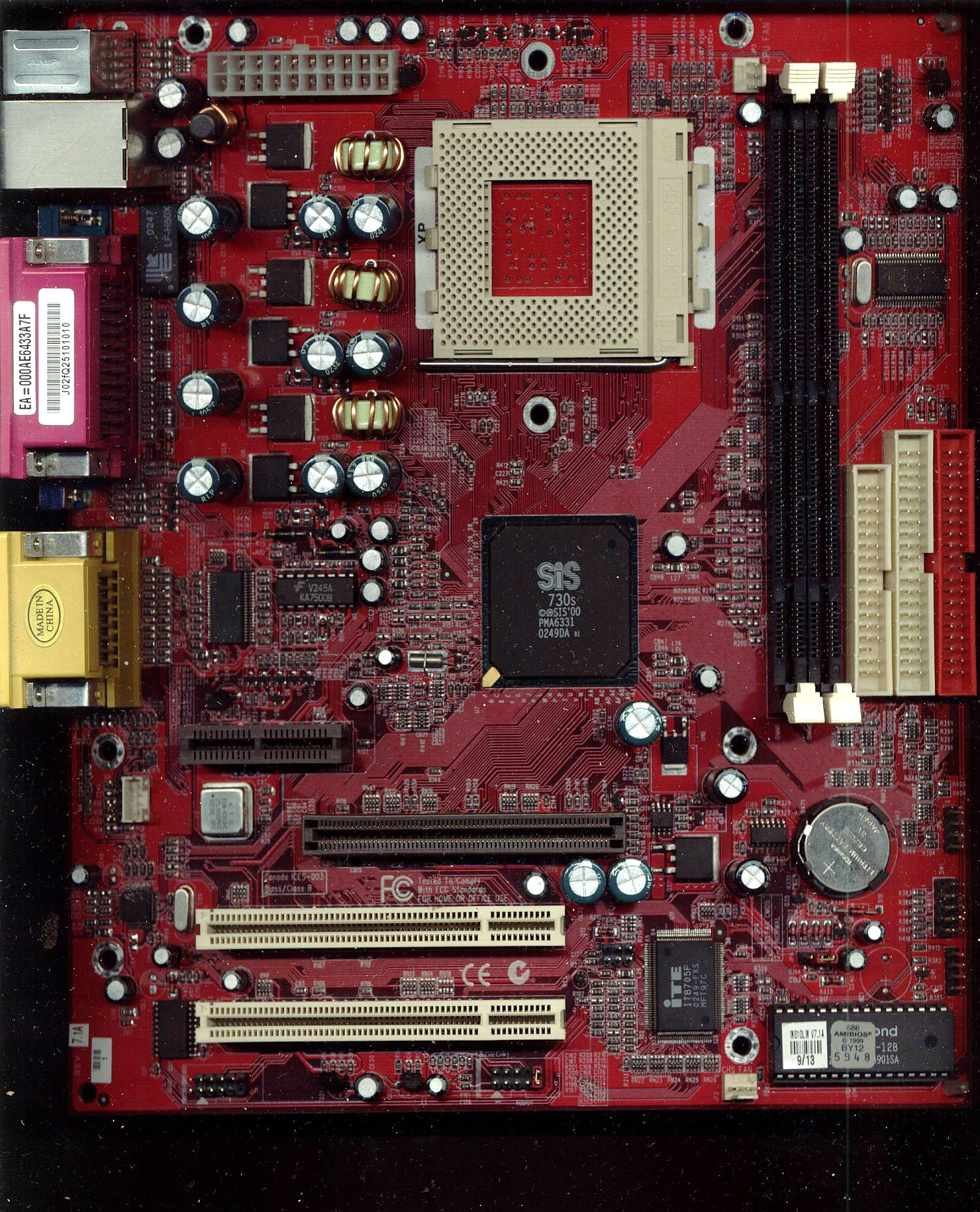 Now what could this be? From a starting point, we know:
1. SiS 730s (which was under a completely blank passive heasink) 2. Poor component layout and what the hell is that AMR doing above the AGP? 3. VIA VT6103 fast-Ethernet PHY when the SiS 730s has one built in. 4. Very high revision number (bottom left) of 7.1 The component layout is a hallmark of ECS but the very high revision number isn't. Back then, ECS didn't design motherboards, it was a contract manufacturer: It just manufactured (and very well I might add) for other entities, providing manufacturing for the likes of Intel, Dell and most top-tier OEMs as well as extra capacity for top-tier motherboard makers like Asus and MSI. Our next clue is from that ECS didn't design motherboards. It had had just bought a company that did...the infamous PC Chips, maker of the World's Worst Motherboards. Have a look on the BIOS chip, bottom right. "M810LM V7.1A" (and a V8.0 is known). This naming style is PC-Chips! Yes, this is the PC Chips M810LM, perhaps the worst Socket A motherboard ever made, tied only with the ECS K7S5A (which was designed by PC Chips too). It's no surprise that this board came out of a dead PC which I'd diagnosed to a faulty motherboard and neither is it a surprise that it took some detective work to identify it as PC Chips; They know they have a bad name. A PC Chips/ECS board will work, but not quite right, never quite stable and eventually it'll just crap out completely. Their ONLY redeeming point was that they were VERY cheap. In 2001, when you could pick up a very overclockable Duron 650 for £15, one of these motherboards for £20 and 128MB of PC133 for £20, all you needed to do was add a £25 15GB hard disk, drop it in a £20 mini-tower with some ungodly nasty "300W" PSU and you had a full working system for £100! Wouldn't work for too long, mind, but long enough to sell and for you to catch your 11 pm flight. See the two holes above and below the CPU socket? Two holes is all they are. They don't correspond to AMD's heatsink mounting specs nor to anywhere a screw should be on an ATX motherboard. See the white plastic stickers saying XP on them? That's all they are too. The SiS730s was never qualified to run Athlon XP, but so long as your BIOS knows about it (SSE required new CPU mode support), Athlon XP would work fine. SiS740 was needed for official Athlon XP support. However, such minor things as "support", "specifications" and "reality" had never stopped PC Chips' marketing in the past. Absolute trash and not even comparable to the similar Asus A7S-VM which also used the SiS730s, same size, but without the AGP and with four PCI slots...but who'd use AGP video with a board like this? The question, then, is why? There's too much weird here for it to not be something different. There's a PDF manual which goes to great lengths to avoid mentioning who made this board. The manual claims the only CPU supported is the AMD Duron. Most likely this was an OEM design but whichever OEM it was for didn't specify the design had to be exclusive, or, perhaps (and knowing PC-Chips' legendary disdain for laws) a ghost-shift line snuck out of a back door at the factory. The M810L (v9.0m) actually had onboard RAM, 256 MB soldered directly to the board! There were several of variants of this base design, M810, M810L, M810LM, M810LMR, and each had as many as ten different revisions. They compete among themselves to be the least reliable, cheapest, nastiest, Socket A motherboard. CPU support: Athlon, Duron Best with: Salt and holy water |
|||||||||||||||||||||
|
Asus A7N8X-X The -X variant of the successful A7N8X series (nForce2 400) means it's the middle-of-the-road model. There's no onboard IEEE-1394 or serial-ATA such as with the A7N8X Deluxe but onboard ethernet and four mounted USB2.0 ports are present, with headers for four more USB2.0 ports. It used Asus' then trademark large passive northbridge heatsink (also seen on the A7V8X) to avoid low clearance fan reliability problems which plagued other motherboards after the first year. In general the A7N8X-X is a typical Asus motherboard. Stable, well built, a little temperamental, all the expected features and some minor compatibility issues. It had the mounting holes and enough socket clearance for the largest of Socket-A heatsinks, the gargantuan (and ferociously effective) Alpha PAL-8045. The good ends there. The BIOS was poor, unable to set CPU voltage below 1.65V (standard voltage for AthlonXP). It hated Crucial Ballistix memory, killing two 512MB PC3200 modules in quick succession. nForce2 chipset boards were known to be very picky about RAM. Overclocking performance was unimpressive, the board was unable to pass 420MHz on either the FSB or RAM, which was with a better cooler on the northbridge and high quality memory. This board powered the servers when they were still on the main workstation and eventually became an AthlonXP 3200+, Radeon 9700 and 1GB RAM system which it remained as a secondary PC and was still quite capable until around 2010. It would run Windows Vista quite well, and even ran Windows 7 reasonably well, but 1 GB RAM was not the same in 2010 as it was in 2005. Socket A came to full maturity at this point. The FSB was running at 400 MHz (200 MHz DDR), RAM was running at 400 MHz, PC-3200. AGP had matured to 8X and 2.1 GB/s transfer rates. All motherboards by this time claimed AGP 3.0, but rarely were. AGP 3.0 was a 0.8V signal spec, which broke backwards compatibility with cards expecting 1.5V signalling. Every AGP 3.0 card was a 1.5V AGP2.0/3.0 universal, and every motherboard was the same 1.5V AGP2.0/3.0 universal. CPU support: Athlon, Athlon XP, Duron Best with: Athlon XP 2500+ at 3200+ speeds |
|||||||||||||||||||||
Asus A7V8X-MX SE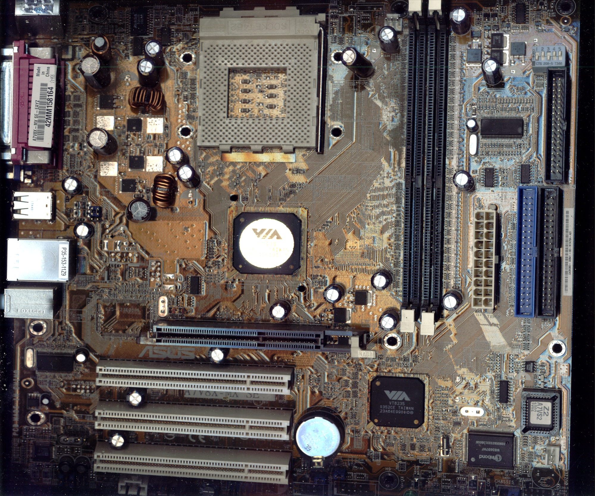 Based on the VIA KM400 chipset (KT400 with integrated video), this is everything an entry level integrated motherboard should be and nothing it shouldn't. It's not meant to be upgraded, just put in a system and left to run. The image is poor and looks very odd, the board was too wide for my scanner and too high, but shows off most of the features of the board. Three PCI, four rear USB, positions for two more USB, two DDR SDRAM slots, three PCI, AGP 8x and the Socket-A ZIF socket. It was the standard square mini-ATX to fit in smaller tower cases and came with a large passive heatsink on the KM400 northbridge the same as the A7N8X-X did, so no unreliable low-profile fan.
Due to one capacitor near the CPU socket, 80mm coolers can't be used, such as the PAL8045. In all, a decent enough cheap low-end motherboard with onboard-everything. CPU support: Athlon, Athlon XP, Duron Best with: Athlon XP 1700+ or Duron 1.4 GHz |
|||||||||||||||||||||
|
Asus A8N-VM CSM - 2005 Nvidia's many AMD K8 chipsets gave a lot of choice in motherboards. The Asus A8N-VM CSM and A8N-VM looked identical, but within the chipset lie a small difference. The A8N-VM CSM is based around the Nvidia GeForce 6150 and nForce 430 MCP, offers one PCI Express x16, one PCI Express x1 and two PCI slots, as well as four DDR DIMM slots, all populated with 512 MB modules in this example. Audio is provided by the Analog Devices AD1986A 5.1. 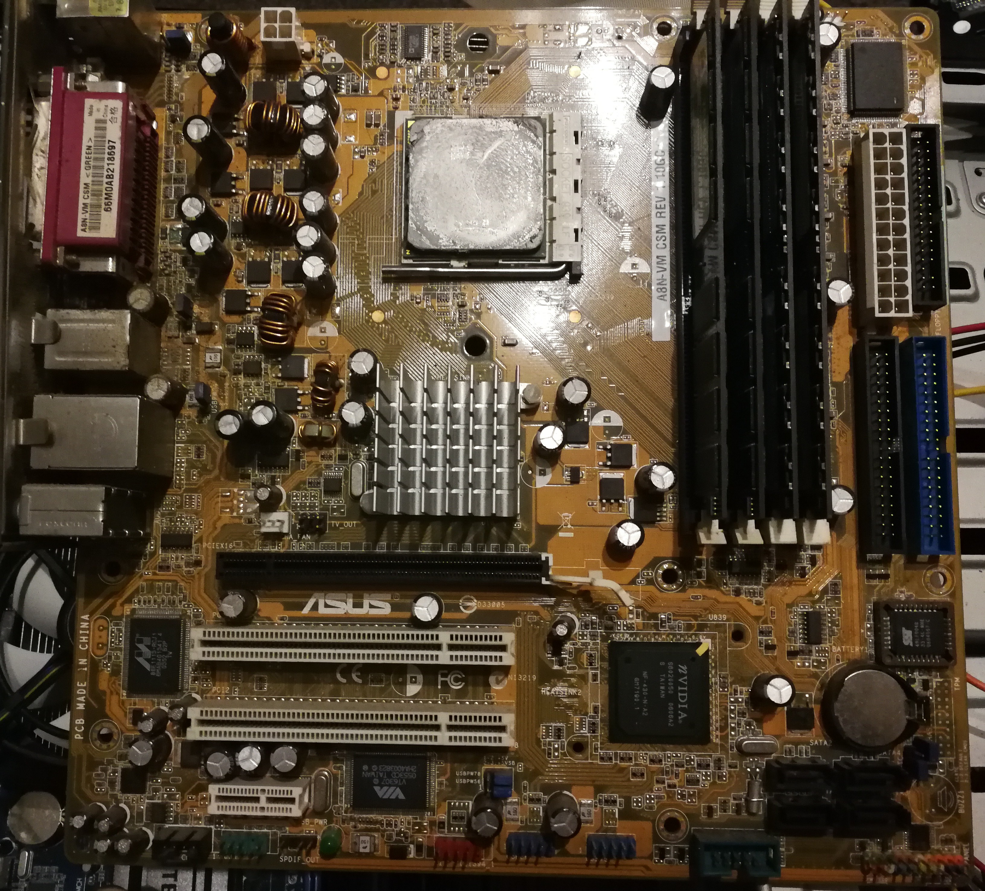 The A8N-VM used the Nvidia GeForce 6100 and nForce 410 MCP. They were exactly the same silicon, so perfectly pin compatible, meaning the same board design can be used for both. nForce 410 disables the onboard gigabit ethernet, so Asus added a Realtek ALC8201. Two of the serial ATA ports are disabled on the 410, so they're simply not fitted to the A8N-VM.
The second difference was the GeForce 6150 and GeForce 6100. Here the difference is even smaller. The 6100 clocks at 425 MHz, while the 6150 clocks to 475 MHz. The 6100 enables only a VGA output, while the 6150 can also handle DVI and component. Finally, the 6150 has a video decoder able to handle high definition media. The GPU integrated is a stripped down NV44 (NV44 was GeForce 6200), and the chip holding it is the Nvidia C51, belonging to the nForce 4 family. C51 was intended for lower cost, highly integrated systems and notebooks/laptops. It has two pixel shaders, one vertex shader and two pixel pipelines in both 6100 and 6150 configurations nForce 4 was the last Nvidia chipset anyone was likely to see, however Nvidia made three subsequent lines on AMD processors, nForce 500, 600 and 700, then dropped the nForce brnading for two more chipsets, GeForce 8000 and then nForce 900 (A rehash of nForce 700). Intel chipsets from Nvidia stopped at Core 2 level, as Intel was unwilling to allow competition in the chipset space for Nehalem and onward. Nvidia did not make an AMD FX chipset and exited the chipset market in 2010. Class action lawsuit later, Nvidia took quite a hit against the GeForce 61x0 series. The chipset northbridge used a poor solder formulation, causing its BGA solder balls to detach from the motherboard. Back to the board. This one has the AMD Opteron 165 (from the CPU section!) fitted, 2 GB RAM, and was running Windows 7 as a home-office machine until 2016. It's still quite functional, simply obsolete. CPU support: Athlon 64, Athlon 64 X2, Opteron Best with: Athlon 64 X2 or Opteron dual core |
|||||||||||||||||||||
|
Asus A8NSLI Deluxe A very high end motherboard based around the NForce4 SLI chipset, this was paired with the Opteron 165 in the CPU section. Alas, my overclocking ambitions were somewhat limited by a chipset which wasn't at all happy beyond 300MHz (giving a CPU clock of 2700, far beneath what even the worst Denmark Opterons were capable of). In attempting to fit a better heatsink to the chipset, a mistake was made and the chipset took fatal damage. The slight chip in the top left corner killed the motherboard.  With two ATA, eight SATA, three legacy PCI and four PCIe, this was a motherboard designed for flexibility and power. The board did have some small oversights, however. The fan PWM controller could only control the CPU fan (the chipset fan was linked directly to it) and the first chassis fan (bottom right corner) and even then, the chassis fan would only be controlled in software such as Speedfan. The fan headers near the PCIe x16 slot and just above the CPU socket had no control at all.
When an overclock failed and the system wouldn't POST, most motherboards would reboot to default settings but 'remember' the failed settings so they could be modified. The A8NSLI Deluxe required clearing CMOS with a jumper under the bottom PCI slot, a location very difficult to get to if all three PCI slots were populated. These were oversights and omissions we did not expect from a motherboard at the top end of things. Nvidia's nForce 4 SLI chipset was meant to be its top of the line, but it had severe issues, to the point of some of its features being completely non-functional. The "ActiveArmor" hardware firewall practically didn't work. High network traffic (e.g. BitTorrent) could cause it to crash the entire system, it would corrupt large transfers, and Nvidia ultimately recommended users did not use this feature. nForce 4 was also not happy with the PCI bus. PCI was implemented as a bridge from PCI Express, but at a lower priority than PCI Express, so if intensive bus traffic to the video card was happening, PCI would violate its latency timer and a device wanting attention would not get it. Finally, nForce 4's SATA-III interface (3 Gbps) was unstable. Dropping it back to SATA-II (1.5 Gbps) would usually remediate this. So, most of the upsells for NF4 Ultra and NF4 SLI didn't actually work! The final upsell from NF4 Ultra to NF4 SLI was the SLI chipset being licensed for SLI. Yes, Nvidia tied this to the chipset for no reason at all! You could enable this license on NF4 Ultra by adding a single zero-ohm shunt resistor on the chipset package. An ordinary soft pencil could bridge these traces and turn NF4 Ultra into NF4 SLI. Without the "SLI license", Nvidia's drivers would "kind of" enable SLI, but one video card was in PCIe x16 mode and the other in x2 mode. With the pads bridged on the chipset package, you got x8/x8 mode. This was worth about 7-10% in performance. The SATA ports are badly positioned (why aren't they were that barcode sticker is?), Asus only know what the ATX power connector is doing all the way over on the other side of the motherboard when it should be on the top edge and the stock fan for the chipset was on an extremely poor heatsink, necessitating a very loud fan. When working, the A8N series of NF4 motherboards (all this design) were good and fast and stable. When being worked on, tweaked or pushed to limits, they were not happy with it nor fun to work with. Not what a high end motherboard should be. CPU support: Athlon 64, Athlon 64 X2, Opteron Best with: Athlon 64 X2 |
|||||||||||||||||||||
|
Asus P5E - 2007 This board occupied that curious place at the low end of the high end. Intel's X38 chipset was the latest at the time and brought PCIe 2.0 to the LGA775 platform. The X38 was a version of Bearlake, which was variously enabled or disabled to become P31, G31, G33, P35, G35, Q33, Q35, X38, and X48. The Eaglelake series had no "high end" product, so X38 was renamed to X48 (and qualified officially to 1600 MHz FSB, though X38 had been doing it reliably) for reasons.  Intel chipsets were a huge segmented mess even then, but that's not what we're here for. We're here for the Asus P5E. It was, even for the time, a bit of an unusual product. The "P5E" name is a little less flourishy than Asus was known for, and an awful lot of the options on this motherboard aren't fitted. On a tour of this board, we first start at the top, where the four phases of VRMs are under a small heatsink. Following the heatpipe round we pass a system fan connector and the EATX12V connector. Under this big silver heatsink are four more CPU VRM phases, the heatsink designed to be cooled by wash from the CPU heatsink, so bear this in mind. The copper-coloured (actually anodised aluminium) heatsink continues to the Intel X38 Memory Controller Hub (MCH, to disguise the fact that it isn't, and actually also controls DMA, CPU bus, and PCI Express), which supports both DDR2 and DDR3 memory officially and can work with previous models of Intel's I/O Controller Hub (ICH) but is intended for ICH9. Following the heatpipe to the "AI Lifestyle" block, this is actually the heatsink for the ICH9R. Take a moment to look around the board. It can run a 4-pin CPU fan and then three 3-pin case fans, but options for several more case fans are there. Other missing features are... A rear mounted clear CMOS, power button, reset button, second LAN controller, three optional case fans, three temperature sensors, LED Poster... There's a lot not fitted and the P5E label between the two PCIe slots is some weird wide sticker. Asus silkscreens the name directly onto the motherboard. Stickers with names on them bring back the spectre of fraud. What's this about?! Does this board have some dark secret? Who's hiding behind that mask? 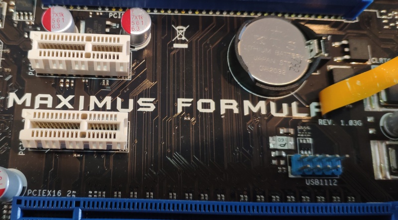
That'll be it! This is actually a Asus Republic of Gamers (ROG) series board, which the SupremeFX II sound breakout (it looks like a sound card, but isn't) alludes to. ROG was fairly new back then and hadn't adopted the modern branding, but only the SupremeFX II even carried the ROG name on this board. Asus considered P5E to have "ROG Level Features". What, then, was the Maximus Formula? Well, it was a P5E with all the missing features not missing! It had a slightly improved BIOS interface too. "Maximus" was the Intel side of the ROG high end boards, and "Crosshair" was the AMD side. We had a Crosshair III Formula (AMD 790FX, DDR3) on the bench (a joy to work with, but faulty) and were aware of Crosshair II Formula (nForce 780a SLI, DDR2) and the original AMD ROG board was just "Crosshair", an nForce 590 high end board from 2006. So why would Asus make a P5E from castrated Maximus Formula boards? It's unclear. Most likely the downturn in 2008 led to Asus having too many Maximus Formula boards in the pipeline for market conditions (Intel X38 was painfully expensive), so decided to cut some of them down. Maybe the adoption of DDR3 (P5E3 and P5E3 Deluxe were DDR3 versions) was slower than Asus liked, but Asus did not have suitable design to extend DDR2 into 2008 and 2009 and cared not to make a new one, instead adapt an existing one. Intel's X38 was released with DDR3 support, the transition was already well underway. Like all Asus ROG boards of this era, and a few years later, the sound is on a breakout card. Let us be making no mistake here: This is not a sound card. It's the Analog Devices AD1988B HD Audio codec, implemented fairly well, but doesn't need to be on a breakout card to do this. Also, the black slot that looks like a PCIe x1 slot is a black slot which the SupremeFX II will only work in, this is because it is a black slot that looks like a PCIe x1 slot. It is not fully a PCIe x1 slot, as it carries the Intel HDA host bus. What did we do with enthusiast level boards of this era? Well, we put E6600s or Q6600s on them and overclocked the snot out of them. This example came out of a large Coolermaster case, with a 650 watt modular PSU, 8 GB DDR2, and a GeForce 8800 video card. The CPU was the then-essential Core 2 Quad Q6600. It'd run bus speeds up to 1600 MT/s (400 MHz bclk), DDR2 up to 1200 MT/s (600 MHz) and came with a wholly passive chipset and VRM heatpipe cooler. This layout was shared with other variations of this board: The Maximus Formula and the Rampage Formula (X48-based, but it's not exactly much different). Other P5E-named boards, such as the P5E WS PRO and P5E-VM were not the same board design. The P5E was so similar to the Maximus Formula that it carries the same name and uses the same BIOS. CPU support: LGA775 Pentium 4, LGA775 Celerons, Pentium-D, Core 2 Duo/Quad/Extreme Best with: Core 2 Quad Q6600 or Core 2 Duo E6600 |
|||||||||||||||||||||
|
Gigabyte GA-MA69G-S3H - 2007 After acquiring ATI, AMD had a chipsets division. This chipset is the ATI RS690 or simply, the AMD 690G, an evolution of the RS485, and pin-compatible with it. Onboard it features a Radeon X1250 (actually on the R300's tech level, not the R420's), but it's more conspicuous for what it lacks: No ethernet! AMD's southbridges did not gain ethernet until the AMD 800 series: The SB600, 700, 700S, 710 and 750 did not support ethernet! The video isn't bad, though. It's about half the performance of a Radeon 9700 (from 2002!) which puts it in line with the Geforce FX 5600. It has onboard HDMI (and a DVI dongle for it), a VGA connector, still important in 2007, and doesn't need one of those ungodly whiny fans on the Northbridge, just a small passive heatsink. The IGP identifies as "Radeon X1250" which puts it right against Nvidia's Geforce 6150. The Geforce 6150 is built into NV's NForce 430 chipset, so how do they compare? GPU Core Clock Arch. SM X1250 RV370M 400MHz 4x1 2.0 (4x pixel, 0x vertex) 6150 ~NV43 475MHz 2x1 3.0 (2x pixel, 1x vertex)ATI say that the GPU is half the RV410 in the X700 but the GPU has no support for pixel shader 2.0b, this makes it in the R300 (Radeon 9700) descent, not from the rework to R420. It is architecturally almost identical to Radeon 9800 SE, X300, X550 and X1050. R420 decoupled the shaders from the ROPs, this does not have such decoupling, so it is not a derivative of RV410. Instead, it's a version of RV370 (X300, X550, X1050) and quite old. A quick session of Oblivion revealed the video performance to be, well, a little lacking. On Medium settings at 1280x720, it ran very badly and struggled to top more than 10 FPS. Even on Low, frame rate didn't often break 20 FPS. It would run Vista and Win 7's desktop fairly well, and that's about it. Of the ten possible USB2.0 ports, it has four on the back and headers for six more, this is good as it's utilizing the chipset's available features. It adds three IEEE-1394 ports (two headers, one rear port) courtesy of a Texas Instruments 78AF5RW, one has to ask why? Surely the board space would be better used in adding an ethernet controller than adding four channels of a dead technology? Instead, we're stuck to a single Realtek 8110C gigabit ethernet when almost every other board other than bargain basement nothings can sport dual gigabit. Where the second ethernet port would be on the back is an IEEE-1394 port. If we want it, we'll add the headers ourselves! About a year into the operation of this motherboard, the onboard ethernet disappeared. Plain wasn't detected as present by any OS and the "smart cable detect" in BIOS just hung.  The port layout and the ridiculously out of place IEEE-1394. It wasn't clear who this board was aimed at. Quiet PC and HTPC people wouldn't go for it, it can't even control the system fan (but SpeedFan can do it), meaning the onboard media capability and HDMI is irrelevant. Gigabyte's own GA-MA69VM-S2 would be a better choice anyway. Gamers wouldn't care about having the onboard video at all. Oh, and it worked with a Phenom II X4 955, but only at 800 MHz. This is because the board has single plane power and while the board is rated to 125 watts, AMD's AM3 processors require dual power planes at 125 watts and will clock down to 800 MHz if they detect a board without. By hammering the FSB (HT clock) I was able to get a working quad core 1,400 MHz system. Not too shabby, but soon replaced. The motherboard is one of many which have run the server hosting this website, and it was the incumbent from 2012 to 2015. It was sold soon after it was replaced by a HP Microserver. CPU support: Athlon 64 X2, Athlon X2, Phenom, Phenom II, Sempron Best with: Athlon X2 |
|||||||||||||||||||||
|
ECS MCP73PVT-PM(SN) - 2009 Well that's a heck of a name. This came out of a Packard Bell where the motherboard had subtly failed. It came to me (in 2019) with a failed video output. Removing the video card (A Zotac GT 620 1 GB) and using onboard video (GeForce 7100) worked, and it wasn't a heavy gaming system, so it was sent on its way. Not long after I discovered that the video card was actually fine. However, no amount of configuration in BIOS would get the IGP to disable, and no video card tried would actually be recognised. At this point, it appeared the PCI Express slot had failed. Ten years out of a motherboard is pretty good going, and I'm not holding anything against it. It spent its life running a Core 2 Quad Q8300: Far too much CPU for this motherboard! The spec was like that from the factory, Core 2 Quad Q8300 and 4 GB of DDR-800 (PC2-6400) RAM. A decently fast 640 GB hard drive made up the numbers but, but... oh, but what about the motherboard? Here, Packard Bell dropped the ball. A better system would have used a Core 2 Duo, the MCP 650i or Intel Eaglelake chipset and pushed the cash saved from not using an expensive quad core into either a video card (e.g. Nvidia GeForce 9400) or a better motherboard. 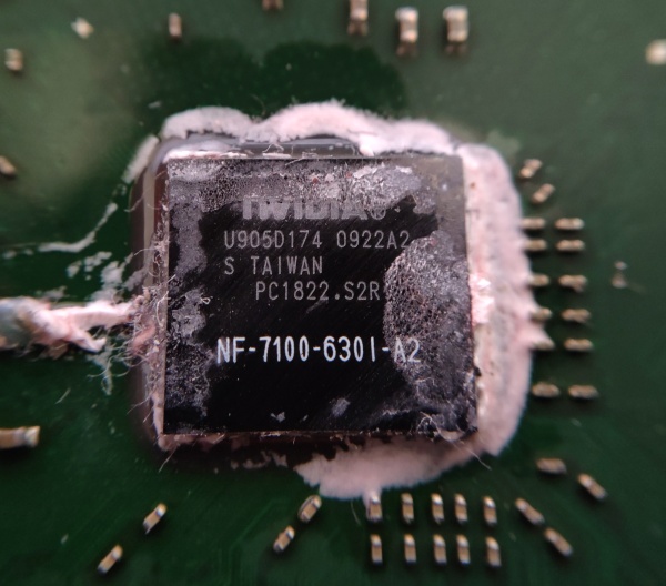 The core chipset is the nForce 630i/GeForce 7100/MCP73. The board, for the day, was very, very basic and extremely low-end. Nvidia seemingly couldn't think of a name for the chipset (the chip is the MCP73) and referred to it as NVIDIA GeForce 7100 or nForce 630i, the lowest end Nvidia chipset offered on the Intel platform. nForce 650i and 680i were the higher end ones, each of which had "Ultra" and "SLI" subdivisions. 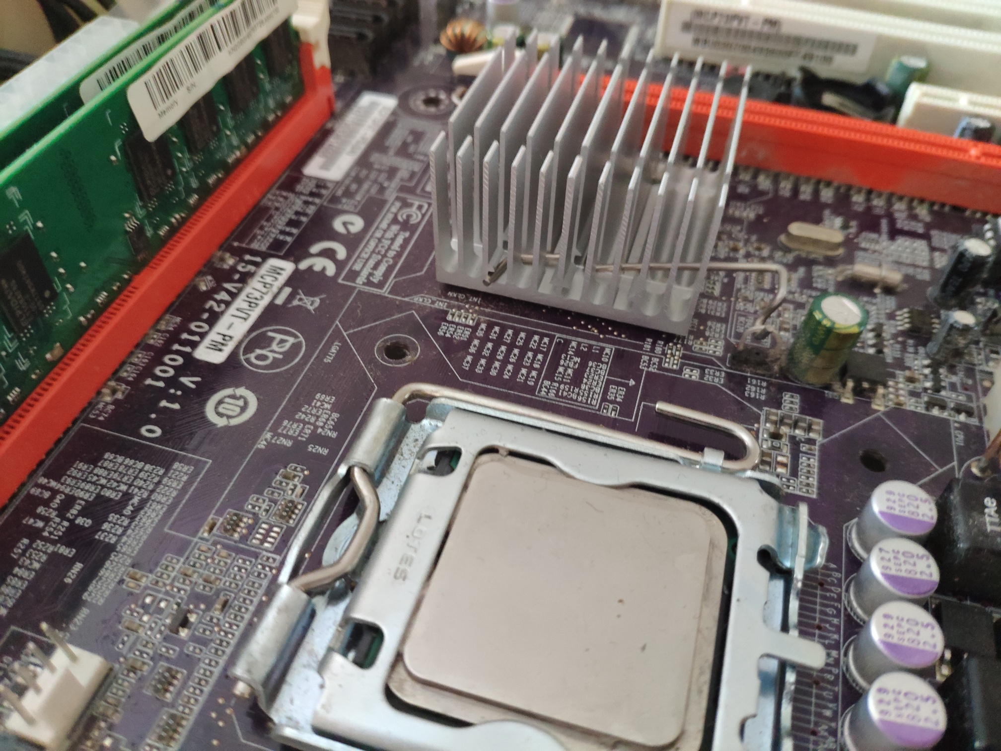 A big limitation, which dragged down performance of this chipset, was the single channel memory. Onboard video has always been enormously bandwidth limited and a single DDR2-800 channel offers 6.4 GB/s only, not even enough to keep the CPU (which was a quad core, high end for the day!) happy. With the CPU and IGP both fighting for very limited bandwidth, this was not going to be very quick. Core 2 Duos saw improvement going from single to double channel RAM, Core 2 Quads saw even more improvement.
Intel's competitor here was the G41 Eaglelake chipset, which was hard-limited to 4 GB RAM, but at least dual channel. 4 GB was about right in 2009, so no points lost there. nForce 630i was not limited, and would use 2x 4GB modules if it could get them. I never saw such a module in the wild. 1GB and 2GB modules were common, as were 512 MB modules early in DDR2's life. Still, 4 GB and four cores is an acceptable light duty box even in 2020. This may get Linux installed on it... What of the board itself? ECS is, of course, the industry's lowest bidder. However, they're also one of the largest contract manufacturers in the world. Design is done in Taipei, manufacturing in Shenzen and Suzhou in China, and Juarez, Mexico. Is this board well designed? Yes, it actually is. It can be criticised for lacking features, but it has reasons for nearly all of these. Only two RAM slots: That's all nForce 630i supports. Only one PCIe x1, and fouled by a dual slot video card? Yes, because two PCI slots was standard and more important in 2009, no way to fit those on a micro-ATX and not foul another slot with the video card. Component layout is very good, nothing fouls the CPU slot for large heatsinks, the ATA-40 header is out of the way, the ATX power connector is in a standard (but still annoying) location. It uses 3 phase power (but with only 3 MOSFETs per phase, one MOSFET is not fitted). Audio is Realtek's ALC885, Ethernet is Realtek's RTL8101E, both of them well regarded. Four USB make up connectivity (dual PS/2 also), with video output being VGA or HDMI. Most machines did use only one monitor, and HDMI is easily convertible to DVI, but it still would have been nice to see the DVI port fitted: The silkscreening is there for it. The silkscreening is also there for the IEEE.1394 controller just behind the PCI slots, which is an easy cut to any motherboard. For the money, it was right in the middle of what you'd expect. It's low end, cheap, and fairly decent. It makes compromises to get the price down, but ones we can live with. A low end or value segment board has to have as much as what you do want as possible, and nothing you don't want. It's not there to be clever or innovative, it's there to get down to work. When doing this approach ECS has historically been quite successful. Four RAM slot machines of this era, with Core 2 Quads, can easily be made up to 8 GB usually (e.g. nForce 650i or 680i) and make really quite usable Windows 10 machines, even if Windows 10 doesn't officially support them. With a SATA SSD and a light video card, they'd still pull their weight against the Pentiums and Celerons of ten years later. CPU support: LGA775 Core 2 Duo/Quad Best with: Core 2 Duo E6600 |
|||||||||||||||||||||
|
MSI 790XT-G45 / MS-7388 / K9A2-CF - 2009 MSI was not great at names. Here we see a fairly typical AM3 desktop motherboard with an original AMD stock heatsink fitted, the type before AMD branded them as "Wraith", which were supplied with Phenom II and early AMD FX processors with TDPs up to 125 watts. This particular one appears to be the older AM2+ variety, supplied with earlier Phenom II X4s. The later AM3 version was not as good, but close. Either heatsink is fine for either socket, we merely lacked a good name to distinguish them. 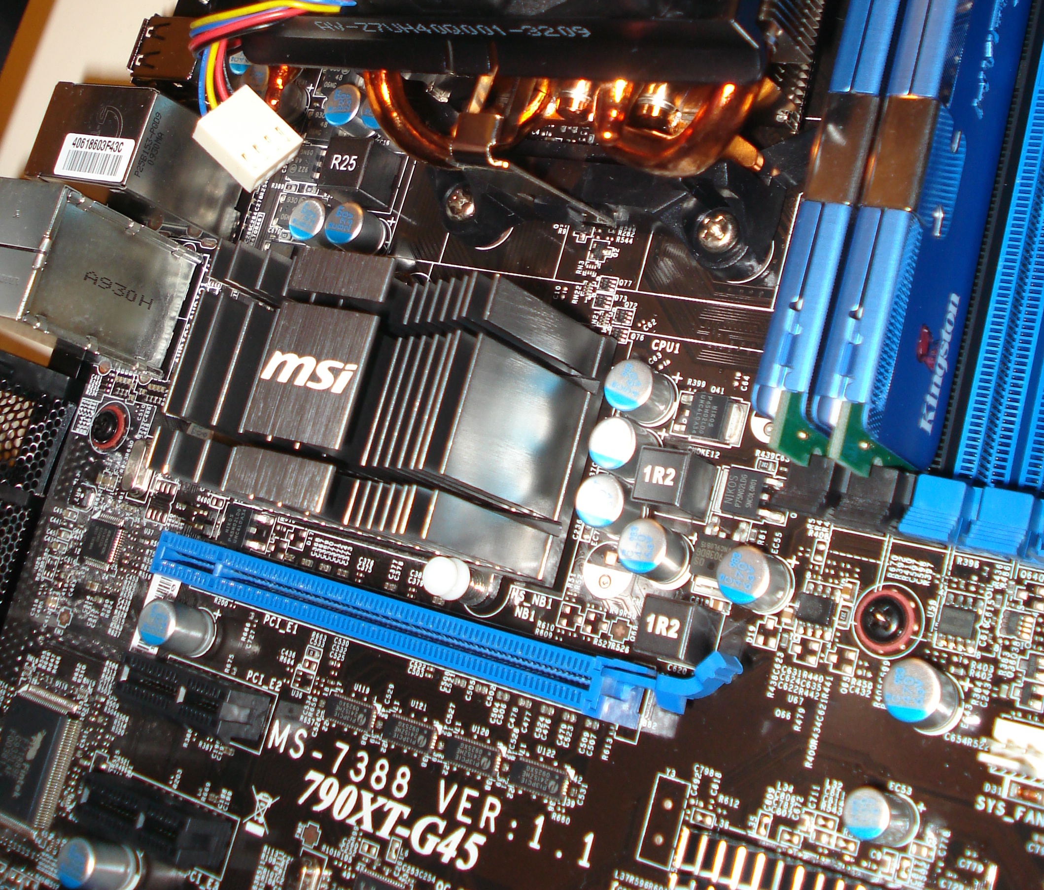 Now then, what's going on with the names here? K9A2-CF was version 1.0 of the MS-7388 and had a rather unfortunate flaw in its handling of high power CPUs, namely, it was likely to be slightly unstable with 125 watt CPUs running on the edge of their capability, such as in cramped and hot cases, as the VRMs lacked any cooling at all. MSI removed 125 watt CPU support from the board, after selling a bunch of them with 125 watt support. The MS-7388 1.0 was the K9A2-CF, K9A2-CF-F and K9A2-CF V2... Whew!
All this, of course, was because the "MS-7388 1.0" refers to the PCB layout, not anything else. To distance the failed, faulty, fucked boards from the fixed revision, MS-7388 version 1.1 (which DID have working 125 watt support) was given the 790XT-G45 name, added a second PCIe x1 slot, beefed up VRMs, rerouted the PCIe x16 northbridge lanes... it should really have been its own thing. AMD 790X had 22 PCIe 2.0 lanes (and 4x PCIe 1.1 solely for connection to an SB600/SB700 series southbridge) meaning PCIe x16 video card ports could either be in a 16/4 configuration or an 8/8 configuration for CrossFireX use. Later in AM2's life, it became favoured to use PCIe switches instead, so an electrical 16 lane configuration could go to both video cards and the port be switched between them. Just under the PCIe slots are four high density SMD components. These are Peritel P13PCIE series bus switches of the 2415ZHE variety. This tells us "2" for PCIe 2.0 or Gen2, and "4" for the number of lanes which can be switched. Four of them means all 16 PCIe lanes can be switched. The AMD 790X chipset used here was usually seen on AM3 (DDR3 support) platforms, but often on AM2+, which was the semi-official name of the AM2 platform updated with dual power planes and support for 125 watt CPUs. CPU support: AM2/AM2+ Best with: Athlon 64 X2 |
|||||||||||||||||||||
|
Asus Crosshair III Formula - 2009 This socket AM3 motherboard was paired up with a Phenom II X4 955 Black Edition and immediately something was not quite right. The system would power on, but then not proceed to past the POST sequence. Flexing the motherboard by pushing the large CPU heatsink would resolve this, but when running it was never quite stable. 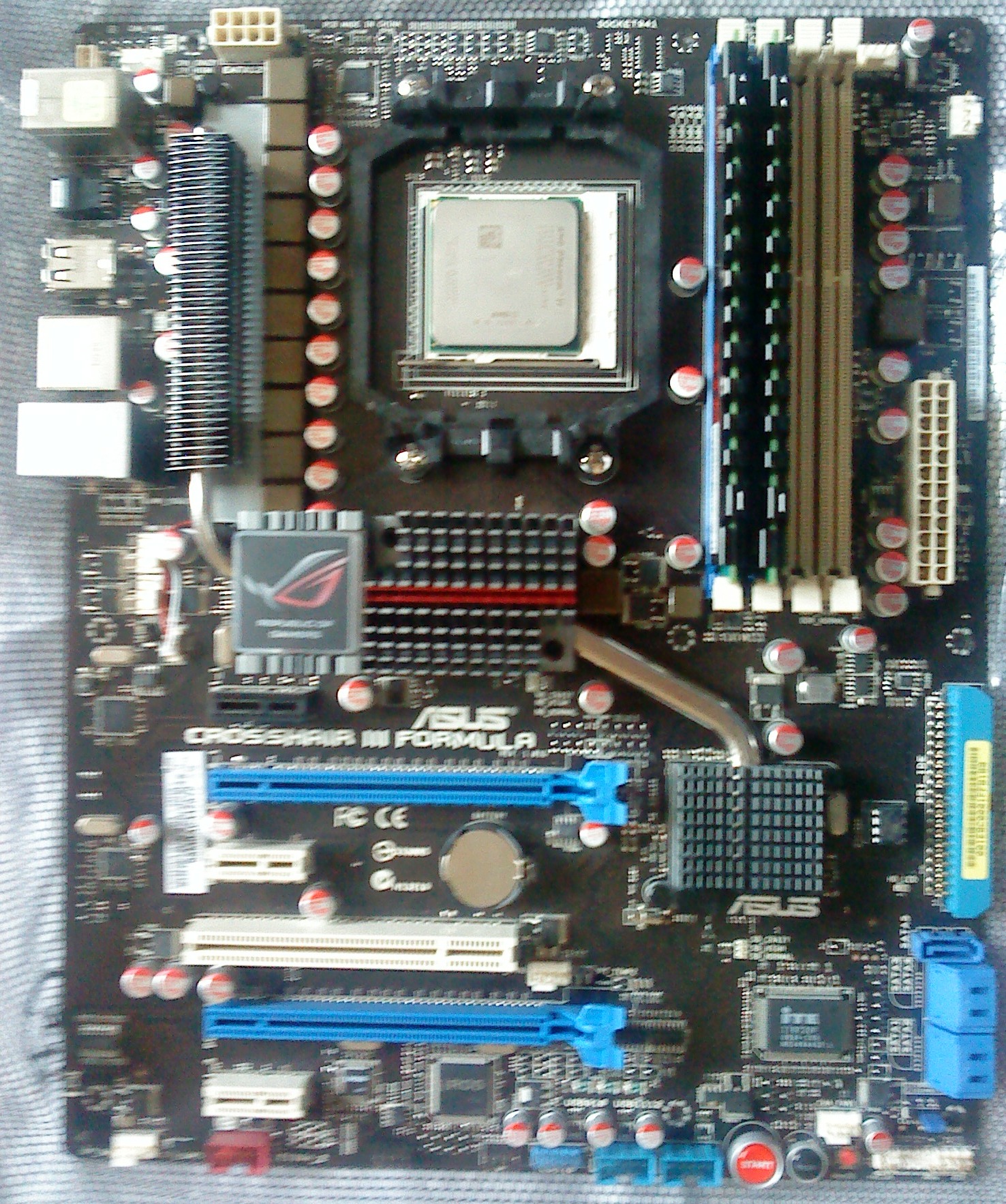 I eventually attributed it to shipping damage, it was likely that the AM3 socket had a flaky connection somewhere.
When running, it was a truly magnificent sight to behold with everything and more (including LEDs everywhere, which can mercifully be turned off). AMD's 790FX chipset, heatpipe motherboard cooling, five SATA slots and a "SupremeFX X-FI" card, actually an Analog Devices AD1989B relabeled as AD2000B and slapped onto a PCIe 1x card when it would have been better off on the motherboard proper. And likely better off as a Realtek, which enjoy much better driver support as well as superior HD audio characteristics. Creative's bundled "SB X-FI Mobo" software added some rubbish to the control panel and an emulated EAX/OpenAL. Joy. On the back we're treated to a button to clear CMOS (!), six fitted USB2.0 and six more able to be added to standard headers (backplanes supplied), a single IEEE 1394a port and a header for another. There are buttons everywhere. Aside from the rear-mounted CMOS reset, you also get buttons to reset and power on the motherboard, mounted right on the motherboard. Asus' "MemOK!" (another button) is intended to smooth over RAM incompatibility problems by essentially brute-forcing RAM timings until one is found which works. Normally, this is the slowest. It can do all kinds of other weird overclocking things, but the only one really worth pointing out is that it can save multiple copies of the entire BIOS set up as profiles, so set it up and save your profile. If you change stuff and it goes south, you can reload a profile and everyone's happy. It also features AMD's "Advanced Clock Calibration", essentially a core unlocker. Through overclocking, steady DDR3 speeds of 1600 MHz are possible and this is clocked cleanly, so doesn't really count as overclocking except the CPUs don't officially support it. On to the ugly. AMD's SB750 has perhaps the world's worst SATA implementation. When the CPU is clocked down due to little load, disk performance tanks. As CPUs are normally under very little load when accessing the disk (as the task is loading, rather than running!) this drags down the entire system's performance. There is actually a noticable difference between the default 800 MHz minimum power state and using Phenom MSR Tweaker to prevent it ever going below 2 GHz. Power draw is higher, of course, but the system is also much more responsive. Asus' chipset cooler, while it looks impressive, actually has a very poor connection to the AMD 790FX northbridge, resulting in temperatures surpassing 90C under load. For a high end board, this was somewhat a worrying lack of attention to detail. It caused me a brief "eureka" moment when trying to stabilise the system, only to discover that even keeping the chipset below 50C didn't help matters. This motherboard can do practically everything except, in my case, work properly. CPU support: Phenom II Best with: Phenom II X4 Black Edition |
|||||||||||||||||||||
Gigabyte GA-EG41MF-US2H Rev 1.0 The unlikely Intel G41 chipset powered a number of low-end boards, Gigabyte had around thirty different models! With Nvidia exiting the chipset business, nothing was there to keep Intel honest, so the market abuses became more and more egregious as time went on. Without competition, Intel held itself back.
The chipset itself was 82G41, Eaglelake-G, and a variant of the G43 and G45 chipsets, however Intel did not make more types of silicon: All Eaglelake chipsets were the same thing and had features turned on or off after production using die-fuses. G41 had nearly everything which could be disabled, disabled. It was a nadir of chipset capability, and the minimum viable product. It couldn't actually have anything else disabled or taken away and still be a sellable product. Why do this? Having a stinker at the bottom of the stack helps justify higher prices further up the stack. It would only talk to the old ICH7 southbridge, but also supported both DDR2 and DDR3. G41, B43 and P43 all had DDR2-1066 and DDR3-1333 disabled, which didn't stop motherboard manufacturers (like Gigabyte) from enabling it anyway, because memory clock is controlled by the motherboard. All Eaglelake chipsets limited DDR2 support to a maximum DRAM density of 128Mx8 (this is the DRAM's presented organisation, which is 128M rows by eight columns, making 1024 Mbit capacity, or 128 MByte. This meant that the maximum reasonable density for a DDR2 DIMM intended to work with Eaglelake was sixteen (eight per side) 128MB chips, for 2GB per DIMM. Eaglelake itself was just a minor update of Bearlake, and G41 replaced G31 in the market. Intel positioned G31 and G41 at the embedded market, not motherboards, and limited it to the ICH7 to help prevent motherboards using it, as ICH7 was very much out of date and lacked a lot of connectivity. Intel charges an awful lot for its more recent ICHs (despite them being virtually free to make), because what choice do you have? It was actually economically viable to use the obsolete ICH7 and simply add on controller chips to the motherboard to patch over its shortcomings or, where the additional connectivity didn't make a difference, to simply make a small ITX board. Audio is provided by Realtek's ALC888, networking by Realtek's RTL8111C - It was cheaper to buy an entirely discrete ethernet ASIC than to pay Intel to enable the present, working, but disabled network controller on the ICH7. A Texas Instruments controller provides the single IEEE.1394 port, which isn't even fitted and instead on a header. IEEE.1394 was virtually free at this point. On G41, RAM could be three "sides" deep, so a double sided DIMM would work alone, or on the same channel as a single sided DIMM. On this board, DDR2_1 and DDR2_2 were one channel, and DDR2_3 and DDR2_4 were the other channel. It was also limited to a maximum capacity of 4 GB. If you wanted more, you paid more for an Eagllake chip with that enabled. Anyway - G41 was a very popular chipset for low end motherboards or small motherboards, particularly with Core 2 Duo or even Core 2 Quad CPUs, reducing the cost of entry to the wallet-assaulting Core 2 platform. Intel intended it for the savagely butchered Celeron chips, but most folk building a system instead went for Core 2 Duos. This particular board was replaced by a Gigabyte GA990XA-UD3 and a Phenom II X4 955 Black Edition, which this writer provided. A few months later, my server (which runs this site) failed with a PSU failure. As a slimline PSU for a HP ProLiant Microserver (with its almost-unremovable sideband SFF-8087 MiniSAS connector) ran far too expensive, I bodged up a Dell 300 watt unit to feed it, and the guy who I gave the GA990XA-UD3 offered to supply this board. The CPU in the ProLiant Microserver, an AMD Athlon II Neo N36L was both quite slow and ran at a mere 1.3 GHz. He originally didn't supply the HSF mounting backplane, forcing the PSU bodge job, and the only heatsink I had was an LGA1155, which has its mounting holes out by around 3 mm (LGA775 is a 73mm square, LGA1155 is 75mm). Thanks, Intel. CPU support: LGA775 Core 2 series Best with: Best avoided |
|||||||||||||||||||||
Gigabyte GA-970A-UD3 Rev 1.0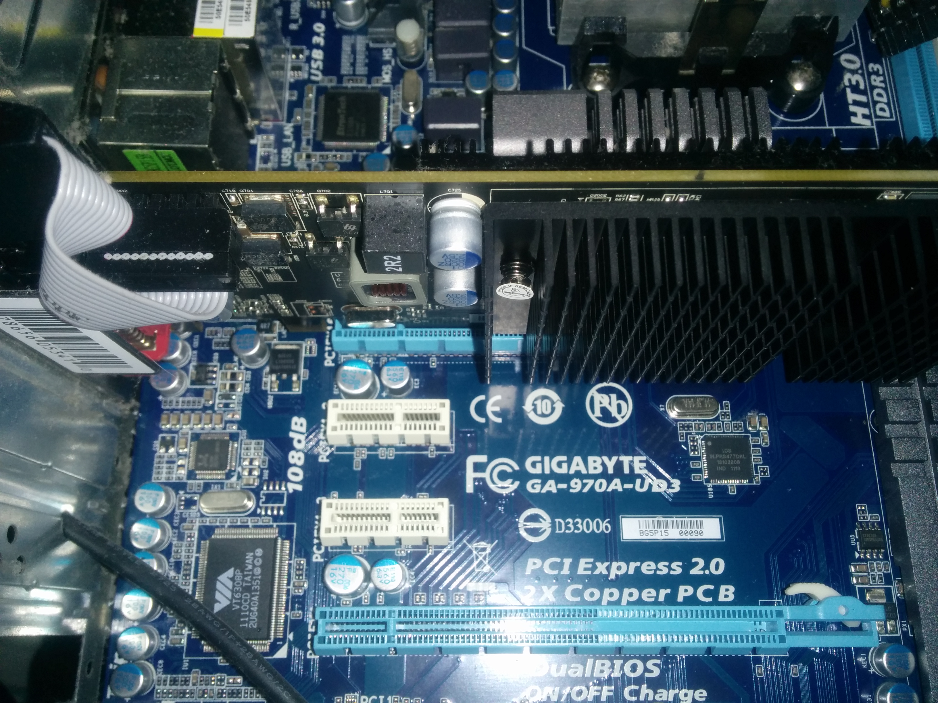 This little thing was paired with a Phenom II X2 550 but, a few years into its life, the owner brought it back, asking for a trade-in for something smaller. Physically smaller, that is.
He had a reasonable budget, so went out with an Intel Skylake NUC, outfitted with a 256 GB SSD and 8 GB RAM. This AM3 board was then surplus so, of course, it was unlocked to the X3 spec (X4 wouldn't work), clocked at around 2.8 GHz if memory serves, and sent once more on its way. The AMD 970 (RX980) chipset was intended to be AMD's entry level, it was very similar to the AMD 990X (RD990/RD980). Technically, AMD 970 didn't support CrossfireX or SLI due to the PCIe configuration being locked to 16x/4x and that was pretty much it. AMD 970 was meant to go with the lighter weight SB920 southbridge, but nothing stopped use of the SB950, which Gigabyte did use here. While CrossfireX was not certified on the AMD 970, it worked, and this particular board did it, with two Radeon HD 5750s. The lower PCIe x16 slot was wired to x8 and connected to x4. The little chip which looks like it may be a PCIe switch is in fact the Renesas/IDT 9LPRS477D programmable system clock generator for ATI RD790/K8 systems and was specified by AMD for use with all its chipsets. CPU support: Phenom II Best with: Phenom II X3 or X4 800 series |
|||||||||||||||||||||
Gigabyte GA-990X-UD3 Rev 1.0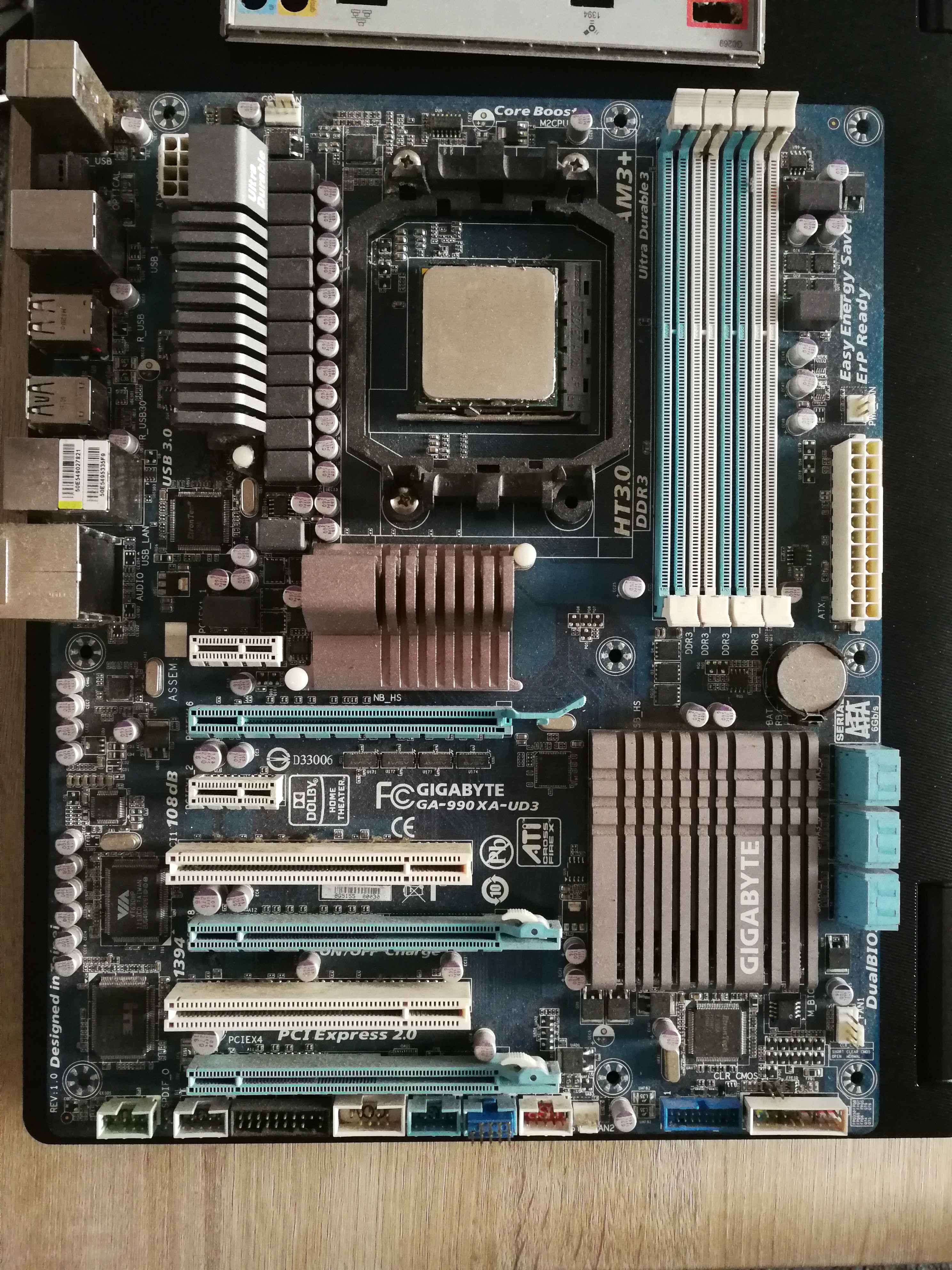 AMD's 800 and 900-series chipsets were not really new chipsets per-se, they were iterations on the 700-series. They followed ATI's naming convention, so the 990X was the RD980 chipset. RD990 was 990FX, and RX980 was the 970. The 990X chipset drops sixteen PCIe 2.0 lanes, but still allows multiple GPUs by using a x8/x8 configuration. 990X also drops four of the "general purpose port" (GPP) PCIe lanes, presenting only 6 of the total 10. The two GPP clusters, six lanes in GPPa and four lanes in GPPb support any mixture of slots from GPPa, such as x4/x2, x4/x1/x1, x2/x2/x2 or even six x1s. The GPPb only allows a single device, so must be connected in x4 configuration. GPPb is, of course, not present in the 990X chipset.
On to the board. The layout of the board is excellent, but for the silly ATX power connector. Like many boards, it blocks drives in cases which aren't as deep as they could be. The PCIe layout of this board was bloody weird for a 990X board. It uses PCIe switches (the four high density chips just below the top PCIe x16 port). The upper port was full x16, but became x8 if the middle x16 port was in use, this is electrically x8. Look carefully, and you see the pins don't reach to the end of the slot. The lower port is wired from, it seems the second block of 8 lanes from the PCIe GFX of the 990X chipset. They go via the switches to the middle port and, also, the lower port, which is a very interesting port. Looking at the picture, you can clearly see the right half of the slot is blank, so it's a x8 slot at x16 size. This is okay, it allows a video card to clip in securely. However, half the contact housings inside the slot are not populated, so the x8 slot in x16 size is wired up to be only an x4 slot! All three x16 physical slots share the same 16 lanes on the 990X. The extra six lanes are wired to, respectively:
Gigabyte is proud of the 108db SNR audio on this, and it aced Rightmark Audio Analyzer. The ALC889 is serious kit, featuring 10 DACs, 6 ADCs, 8 remappable ports, the ability to do full 7.1 and run headphones concurrently with different sources and can handle S/PDIF input and output. It'll also do Dolby DTS, SRS TruSurround XT and is cerfified by Dolby PCEE Program for studio mastering. It's also capable of bit-exact S/PDIF pass through to software. In a double blind test at Tom's Hardware, the ALC889 was not distinguishable from a $2,000 Benchmark Media DAC2 HGC. My experience with some now-very-old Sennheiser HD-202 headphones mirrored this: The ALC889 was transparent. It added and took away nothing from the sound. Oddly enough, I also discovered that the very cheap Sennheiser HD-210 cans do an excellent job for their price. This board was paired with a Phenom II X4 955 Black Edition chip, and tasked to run it as fast as it could. The Deneb C2 stepping ran a little hotter and clocked a little lower than the C3, so I wasn't expecting miracles. I got it stable at 3.72 GHz and managed to boot at 4.0 GHz and an ungodly 1.65V core voltage, which even the Corsair H80 liquid cooler couldn't keep under control. Load temperatures rapidly rose about 90C. At 1.45V and 3.8 GHz, it was just barely able to function, with quite frequent crashes under load. 3.72 GHz was stress test limit for this chip. CPU support: Phenom II Best with: Phenom II X4 800 series |
|||||||||||||||||||||
Gigabyte GA-F2A78M-HD2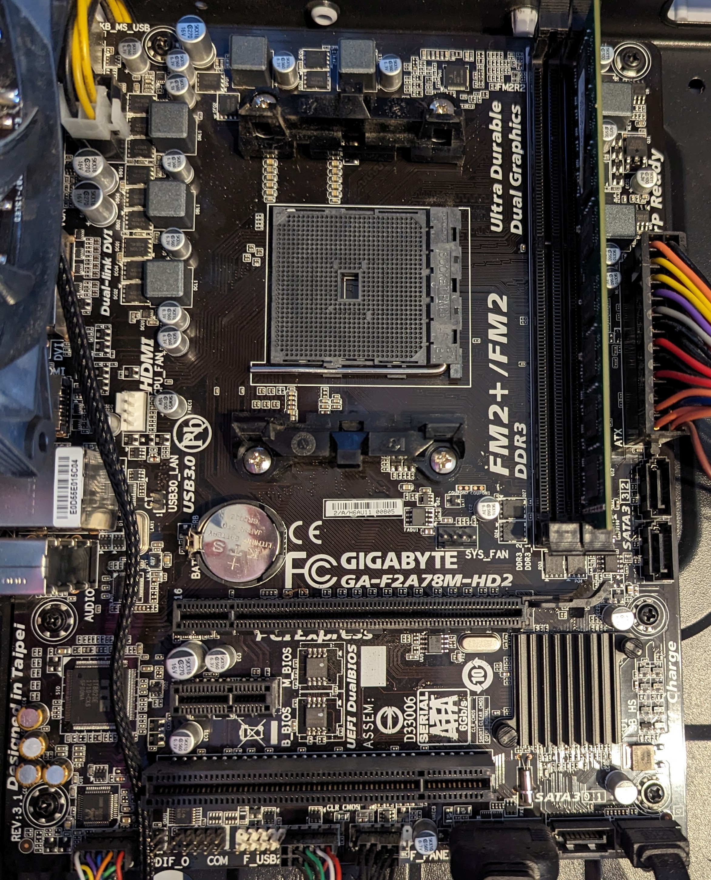
Socket FM2/FM2+ was the immediate ancestor of AM4. AM3 had no facility for video or sound output from a CPU, FM2 did. An FM2 CPU would work in an FM2+ motherboard, as pins were added, not taken away. An FM2+ CPU would, therefore, not work in the older FM2. AM4 is a direct descendant and evolution of FM2+. While it took the "AM" name, it bears far more resemblance to a DDR4 version of FM2+ than it does to a DDR4 version of AM3+. AM3+ was HyperTransport based, while FM2+ (and AM4) was PCIe based. This FM2+ board was too early for that and, well, stuck with a CPU platform which was terrible. This meant AMD had to aim at the low end and that's exactly what this is. There's no heatsink on the VRMs, yet the motherboard supports 95 watt CPUs. There are only two memory slots, a single PCIe x16, a bizarrely out of place PCI slot and four SATA slots. There isn't any M.2 slots here, though in fairness this was before they became popular. The VRMs actually deserve a bit more mention here. There are five CPU VRMs and two RAM VRMs and they're in a really weird layout. Three of the five CPU VRMs are triple-output (a very cheap way of doing it) and two of them are dual-output. The same is going on with the RAM: One VRM is dual-output, the other a single-output. This isn't good. It isn't bad, but it isn't good. The chipset in use here, AMD A78 was one of the "Fusion Controller Hubs", using the "Unified Media Interface" to uplink to the CPU. This was basically a PCIe 2.0 x4 link, almost identical to Intel's DMI, and immediately ancestral to Promontory, which was based around an Asmedia PCIe switch. A78 (and all FCHs of the pre-Zen era) didn't have a PCIe switch, so couldn't add any additional PCIe lanes. This came out of an Athlon X4 880K, GTX 1050 Ti, 8 GB RAM system hawked by predatory scalpers who sold to underprivileged communities on their "monthly cost". The total system price was over £900, for a £400 build! It wasn't even built very well. The fans weren't connected properly, only one DIMM was present, limiting performance, the CPU heatsink (on a 95 watt CPU) had no thermal interface material at all! The system was built back as best as it could be, cooler fitted properly, fans wired correctly, and sent back on its way. Best with: A "For Sale" sticker |
|||||||||||||||||||||
|
Gigabyte GA-B75-D3V Rev 1.0 On the surface, a perfectly ordinary Intel B75 motherboard. B75 is the Panther Point ASIC which was configured as B75, Q75, Q77, H77, Z75, Z77 and C216 on the desktop. Mobile, it was QM77, QS77, HM77, UM77, HM76, HM75 and HM70. In all (desktop) cases, it exposed 8 PCI Express 2.0 lanes, 4 USB 3.0 ports, 6 SATA ports and, in all versions except B75, 10 USB 2.0 ports. B75 had only 8 USB 2.0 ports. Q77 was the "business" or "enterprise" version, so enabled virtualisation (the CPU did this, the chipset was just a flag), while Z75 and Z77 acted as a flag to enable the CPU to allow multiplier adjustment (K-series processor only). This essentially made the primary function of the chipset a licensing dongle! Additionally, Q and B chipsets exposed a PCI bus, and B75/Q75 disabled the second SATA 6 Gb/s port down to 3 Gb/s, giving a 1/5 split instead of the 2/4 split. Motherboard manufacturers rarely made that clear, and this board didn't either. SATA-0 is the 6 Gb/s port. Sound confusing? Which chipset do you need? That's the point. Intel wants you to "not take the chance" and move up, thereby giving Intel a little more money for the same silicon die. Thankfully (and unlike the Sandy Bridge days) all Ivy Bridge chipsets allowed using the CPU's built-in GPU. Only Z75 and Z77 allowed CPU and RAM overclocking, but all the others would allow CPU Bclk overclocking (or, rather, they couldn't stop it) if the motherboard vendor exposed it. RAM overclocking was permitted on B/Q but only to an Intel XMP(tm) memory profile stored on the RAM itself. Intel chipsets a mess? Yes they are. There is no reason for a single CPU generation to have six chipset models, which are configuration variants of the same silicon. Well, no reason except average selling price (ASP) optimisation. This segmentation, which Intel does constantly, keeps prices as high as they will go while not harming volume sales being as high as they will go. Audio on this board, per Rightmark Audio Analyzer 6.4.2, is exceptional. At 24/96, it shows crazy low noise floor (-121 dB at 1 kHz), THD (-71 dB at 1 kHz) and a frequency response dead flat until 20 kHz, when the mic-in (we did the test in loopback) seems to cut off. This is the best onboard audio yet tested (as of June 2020), including the ALC889 implementation of Gigabyte's own GA-990X-UD3, a much higher end motherboard. Gigabyte's motherboard tiering system is fairly simpleLAN is provided by Gigabyte's long-time supplier Realtek, and the RTL8168E stands up the Ethernet here. In my use, it had an undiagnosed problem with jumbo frames being enabled. CPU support: Ivy Bridge, Sandy Bridge Best with: Core i3-2100, Core i5-2400, Core i5-3470 Special Mention: Core i3-3225, Core i5-3570K. These used the fully enabled "GT2" IGP which was, for the time, a substantially effective IGP, and really noticeable on GPU-less systems |
|||||||||||||||||||||
Gigabyte B550 Aorus Elite AX V2 Let's decode that impressive name. B550 is, of course, AMD's B550 mainstream chipset. "Aorus" is Gigabyte's mainstream to enthusiast brand ("Ultra Durable" is the low-end brand), and Elite is the model, a more budget friendly alternative to the more feature-packed Aorus Pro or the high end Aorus Master. "AX" means it's the ATX version not the micro-ATX, so we gain extra PCIe lots and an extra M.2 slot.
Aorus, of course, is Gigabyte's gaming brand, and this is the bottom of the B550 gaming tier from Gigabyte. The "Elite" was the basic, "Pro" was a step up, and "Deluxe" the top of the Aorus line. Howver, it's not an Ultra-Durable, it actually is Aorus level, which means it cannot be a stripped-down bare minimum, so it needs things like 2.5 Gbit LAN, WiFi, an attractive heatsink/shroud design, four RAM slots, dual M.2, a good set of audio connectivity (Gigabyte has always been good at this), RGB controllers, many fan headers, many USB headers and, of course, a feature-rich UEFI. The V2 in the name is the important bit. There was a shortage of many components in 2020 due to COVID-19, and PWM doublers were one such component: Gigabyte couldn't source the ISL6617A part. This forced Gigabyte to have to redesign the CPU VRMs on the Aorus Elite, changing it from a doubler design to a Dual-Output design. VRMs were important in early Ryzen AM4 motherboards, as they were nearly always inadequate for even light overclocking. A simple VRM is a pair of MOSFETs (Vishay SiC641C in this case) which are used to switch current across a diode, which then goes through an inductor (choke) and across a capacitor. The MOSFETs are pulsed on according to a PWM signal. Phase 1 pulses first, then phase 2, then phase 3, etc. all on rising edges of the PWM signal. So the more phases you have, the less each phase has to work, and so the higher each phase's output can be, it's a simple and very effective way of running high current, low voltage, power components.. This pulsing output run through a capacitor and inductor (an LC filter) to smooth it down to the final voltage. Each MOSFET+LC is called a "phase". This board has what Gigabyte calls a "12+2" phase design, so 12 CPU phases and 2 RAM phases. It can be immediately seen that there are not 12 phases on this board's CPU supply. The long row has six capacitors and ten inductors, while the shorter row has three capacitors and four inductors. The number of MOSFETs is hidden under the heatsinks. We have a 6+6 (or 6x2) parallel phase design, according to Gigabyte, which lacks the benefits in low heat of a 12 phase design but offers the same output, albeit if done right. Gigabyte does use 12 inductors, but only nine capacitors. This is known as "Dual-Output", so one VRM feeds two outputs. This sort of thing was overwhelmingly common. Asus' TIF and ROG STRIX B550 boards used dual output, and even triple output. The box features two SATA cables, one compound WiFi antenna, a "G Connector", a driver disc (anyone ever used one of these?) and a printed copy of the PDF user manual. The WiFi antenna reallly should be two with a little horizontal distance between them to take advantage of beamforming. Going through the features step by step, we start with a feature very briefly important in 2020: AMD released Ryzen 5000 series, the Zen3 Vermeer chips. They were compatible with existing motherboards, but a BIOS update was needed. This was great if we had a CPU already, but what if we did not? AMD had a CPU loan scheme, where they'd send you out a Ryzen 3 3100 or a 3300G, but this motherboard can flash its BIOS without a compatible CPU present (it does still need a CPU), as Gigabyte's "QFlash Plus". Asus had similar with BIOS FlashBack. I'm sure MSI had something too, but MSI was behaving very scummy in 2019/20. We next get Intel's WiFi 6 (802.11ax) AZ200 chip, very popular in this generation, which can max out at 2.4 Gbps data transfer, and offers integrated BlueTooth 5.1. Assisting this in networking capability is Realtek's RTL8125BG, which goes up to 2.5 Gbps. 2.5 Gbps, from introduction in around 2016 to the time of writing in very late 2020 was essentially without function. Small 2.5 Gbps unmanaged switches effectively did not exist, while the equivalent 1 Gbps switches were cheap and just worked, and had been for ten years. There are three system fan headers and two CPU headers. Fan control is, to a word, poor. BIOS control is awful, the UI makes no sense at all. App-level fan control is done via Gigabyte's System Information Viewer (why?!) and can link fan RPMs against temperature sensor readings, which are CPU, VRMs, PCIex16, System 1 (lower rear) System 2 (lower front), and PCH (AMD doesn't have a PCH, this is the B550 chipset). PCIex16 is meant to be a proxy for GPU temperature, but for most GPU coolers it isn't in the fan wash so doesn't scale with the GPU. This poor design makes cooling design more complex: There is no direct way to know when a GPU is dumping hundreds of watts of heat into the case! It's best to use something like Remi Mercier's Fan Control for this. Headers for CPU heatsink LEDs and the 5050 compatible addressable RGB LEDs are catered for with two 5V headers and two 12V headers. Internal storage connectvity is two M.2 ports, the upper connected to the CPU's PCIe lanes, the lower to the chipset's PCIe lanes, and the now-standard four SATA ports, two from CPU (upper, near RAM) and two from chipset (lower). It was common for AMD B550 motherboards to be very light on PCIe lanes. The CPU had 24 PCIe lanes, usually configured as 16 to a PCIe video card slot, 4 to an NVMe slot, and 4 to the B550 chipset (really just an I/O expander). B550 hosted 10 PCIe lanes, usually 4 to another NVMe slot, 1 to a GbE LAN, sometimes 1 to a WiFi module, leaving only four left for slots. On this board, they're wired as two electrically x1 slots and one electrically x2 slot. There were no electrically x4 slots outside the single x16 slot! Top to bottom, the PCIe slots were: PCIEX16: PCIe x16 physical, PCIe 4.0 x16 electrical PCIEX2: PCIe x16 physical, PCIe 3.0 x2 electrical. PCIEX1_1: PCIe x1 physical, PCIe 3.0 x1 electrical PCIEX1_2: PCIe x16 physical, PCIe 3.0 x1 electrical PCIEX16 and the upper M.2 slot only allow PCIe 4.0 with a CPU which supports PCIe 4.0. This is the Ryzen 5000 series with the Vermeer or Vermeer-X dies, the Ryzen 3000 series with the Matisse dies but, importantly, the Picasso, Renoir, and Cezanne CPUs do not support PCIe 4.0. Picasso is the Ryzen 3000 APU die, so has onboard graphics, Renoir is the Ryzen 4000 APU die, Cezanne is the Ryzen 5000 APU die. None of these support PCIe 4.0 at all. This includes the Ryzen 3 5100, Ryzen 5 5500, and Ryzen 7 5700, which are all based on Cezanne with the graphics disabled. In my use, PCIEX2 had an M.2 adapter in it for another SSD, which would be limited to around 2 GB/s by PCIe 3.0 x2, but this didn't really make much difference. The chipset's PCIe lanes were used by: 4x CPU uplink 4x PCIe slots PCIEX2, PCIEX1_1, PCIEX1_2 1x Intel AX201 WiFi6 (M.2 E-key slot under the I/O shield) 1x Realtek 2.5 GbE LAN 4x M.2 slot M2B_SB (M-key, can also do SATA) AMD's documentation on B550 is a little misleading here! It says B550 has 38 total PCIe lanes and 30 of them are usable. This includes the 24 total CPU lanes and includes the 4 lanes on both CPU and chipset which are needed to connect with each other! AMD's counting these twice, which I feel is misleading, you don't say a video card has 32 PCIe lanes, 16 on the GPU nd 16 on the CPU! Anyway, B550 has 10 usable PCIe lanes and all ten are in use here, four to PCIe slots, four to an M.2 slot, and one each to WiFi and Ethernet. The rest is pretty much what you'd expect by sight. It's worth mentioning that the DisplayPort and HDMI ports are only active when a CPU containing integrated graphics is installed. It is possible to have these wired such that they'll work regardless of what graphics is installed, but this is very rare and Gigabyte didn't do it here. Gigabyte listed official support only for Zen 2 and Zen 3, the Ryzen 3000 and Ryzen 5000 series. Additionally, it explicitly did not have support for the Ryzen 3200G and 3100G. It supported Renoir, Matisse, Picasso (out of the box) and Vermeer (since BIOS F10). We should probably list that.
BIOS F13 also introduced the AGESA "EDC Bug" which broke Precision Boost Overdrive. This was fixed in F17f. It's worth going into why we now need explicit support for CPUs when a few years before a CPU would work in really old motherboards, even if features were lost. In the early 2010s, the Chelsea Manning and Edward Snowden leaks revealed that the US spy agency NSA had spent a lot of money sponsoring the development of and injection of remote management, including a budget request in 2013 to "Insert vulnerabilities into commercial encryption systems", widely considered to be AMD and Intel. Intel was already in the NSA's good books with Intel Management Engine, and AMD added similar to the AMD FX series. This then needed a BIOS module, AGESA, to load its firmware in. So, just supporting the bus and configuration registers was no longer enough, the "platform security processor" (PSP, also implements TPM) also needed to be initialised. This meant a perfectly working motherboard and chipset also needed BIOS software support to work at all. AMD has repeatedly refused to open source the code that runs on the PSP and Intel will not release code for the Management Engine. Somewhat telling, government agencies can get Intel ME and AMD PSP in "high assurance" mode, where the system is essentialy disabled. CPU support:Zen 2, Zen 3 Best with: Ryzen 5 5600X, Ryzen 9 5900X, Ryzen 7 5800X3D Note on gaming use: The 5600X, 5700X, 5800X, 5900X, and 5950X all had essentially the same gaming performance. Most games would not go beyond six cores (and most wouldn't even get past four) and it then became a MHz race. They are all specified between 4.6 and 4.9 GHz, so there's only 300 MHz in it. More than one amateur PC builder went with a 5900X to get the Ryzen 9 branding, only to realise they were no faster than a 5600X at half the price. |
|||||||||||||||||||||
Machinist E5-MR9A Pro
These guys are sold at ridiculously low prices on Ali Express and they're what I call "Chinaboards". Chinese manufacturers operating with either recycled or new-old stock chipsets have utterly no reason to rely on Intel sourcing them, so they don't need to obey Intel's orders. Intel would never allow the LGA 2011-3 socket on a B85 chipset, even though there's no actual reason why not and nothing was actually stopping it. So, well, here we are. The B85 chipset and an LGA 2011-3 socket, sporting a Xeon E5-2640v3, all for the princely sum of £87, shipped, in January 2024. Oh, and 16 GB of DDR4-2133. I was expecting this to be a somewhat inexpensive time sink. Of course it wouldn't work properly to begin with! So, a similarly cheap SSD (512 GB for £14, under no illusion that's not B/C/Z-grade flash) was imaged with the boot drive for the hattix.co.uk server, a Cooler Master Hyper 212 heatsink dropped atop the Xeon, memory seating quickly checked, CPU socket quickly checked, and it all built up. An Asus Radeon HD 5770 made up the GPU, since the LGA2011s didn't have them. The board is thin, obviously cheaply made, and has a pair of 7 segment displays to give a POST diagnostic, so clearly this wasn't going to work right, but it had the tools to help me out as I found why it wasn't working right. The damn thing booted Windows Server 2022 first time. I wanted this entry to be a good rant about how cheap and nasty crap from Ali Express is barely worth the money or not worth it at all. Instead, I have an eight core Haswell Xeon, which will clock up to 3.4 GHz, supplied with RAM which is actually faster than the processor supports (supports DDR4-1866, supplied DDR4-2133), on a motherboard where all the CPU PCIe lanes are sensibly wired! Both of those X16 slots you see there are directly to the CPU, as is the x4 slot you see. I needed at least an x16 and an x8 for graphics (Xeons don't have it) and the SAS HBA for storage, so that was a key buying factor. The RAM deserves a little mention. This is not high speed RAM by 2024 standards. The SPD doesn't even have a name field, but it is fully populated and has sensible timings. It'll do 2136 CL15, 2036 CL14, 1890 CL13, 1744 CL12, 1600 CL11, or 1454 CL10. This is very clever! BIOS RAM timing selection picks the closest SPD profile above clock it's using. If we're on a 750 MHz clock reference, so 1500 MT/s, we can't use the 1454 CL10 profile, so the 1600 CL11 profile has timings safe to use. By having the profiles all a little higher than common RAM clocks, the memory helps BIOS select the right timings for any clock. If we had a 1866 profile and BIOS thought we were running 1867, we'd probably run looser timings than we actually needed to The timings here are loose. While the DRAMs are identifed as Micron manufactured, they are not top speed chips! The CAS latencies are aimed at 13.75 ns, the tightest actually being the 1600 CL11 profile, which is exactly 13.75 ns. In use here, the RAM ran its 1890 CL13 profile at 1866 MT/s, at 13-13-13-30. For comparison, some Corsair Vengeance LPX memory I have here also has a profile suitable for 1866 MT/s operation, which is 13-13-13-31! It also has an XMP profile too, which would do 10-12-12-23 (the top profile on the Corsair RAM is 3200 MT/s 16-18-18-36). Anyway, back to the motherboard, there is still lots more to say! Both M.2 slots are wired to the B85 chipset. The upper says it is SATA only, but it has no SATA at all, it's full-on NVMe, the lower is NVMe only. Under the upper M.2 is a second M.2, this time E-keyed, intended for a WiFi module. SATA M.2 SSDs will not work in any of these slots. The lower PCIe x1 slot may be chipset connected, or may be CPU connected. The CPU has 40 PCIe lanes and the upper slots only account for 36 of them, so one of the M.2s may be to the CPU, or the four lanes could just be not connected. I'd expect the B85 to be doing the NVMe, as the CPU didn't officially support it but the chipset did. The missing four lanes are accounted for by the top PCIe slot, which is an x4, but Haswell-E could only do x8 or x16, so that slot will always be "pretending" to the CPU to be an x8 slot, with a maximum of a x4 card in it. If a CPU with only 28 PCIe lanes is used, the top PCIe x16 slot is x8, but only the last 8 lanes are active. This violates the PCIe spec, though most x16 cards will work, cards with only x1, x4, or x8, will be wired to the first 1, 4, or 8 lanes. One last PCIe thing I do want to call out here are the slot retention levers. They're great! Big, wide handles, easily pushed when a huge video card is in the way, with a lot of leverage, and they hold the PCIe card well. Moving on, SATA is exactly what you'd expect from a B85/C220 chipset, four SATA 3.0 and two SATA 2.0. As built, only one was in use, for the suspiciously cheap SSD. Storage on this build was handled by an LSI Logic 2008 SAS HBA, purely to take advantage of roaringly cheap refurbished SAS HDDs! They were well cared for previously and nobody wants to buy them as refurbs! The board does not use B85's onboard ethernet, and has a jumper to hard-disable Intel Management Engine. This is very, very typically China. They do not want American spyware at all, and Intel's built in Ethernet has a direct link to the Management Engine which can be used even when the system is powered down. Networking is handled by a Realtek 8168 MAC and 8111 PHY, the actual chip is off under the I/O shield housing, just visible to the left of a crystal oscillator by the RAM slot. VRMs are eight dual-output and with a moderately sized heatsink, and tiny fan to actively cool them. A spare fan is in the package with the motherboard, and a connector for a second tiny fan is given. I wouldn't doubt this motherboard's ability to power 150 watt CPUs, but above that may be a stretch. Dual output VRMs are a cost saving feature often found on mid-range motherboards. The low end just runs something like four or six phases (sometimes also dual output) while the high end will have 8, 10, or 12 single output phases. By doubling the MOSFETs on a single phase, the phase can handle around 1.6-1.8x the power, so four dual output phases aren't as good as eight single phases, but are as good, or better, than six single output phases. Some manufacturers would call this "Eight virtual phases" or, in Gigabyte's case "twin power design". It's easy to check, just count the inductors. They're usually black squares these days. A VRM phase has only one inductor. This motherboard, therefore has eight dual-output VRMs. This is a very solid design! Most of these Chinaboards have four dual-outputs (and not good for CPUs over 90 watts) or six dual-outputs (including earlier versions of this very board) which will be okay up to around 140 watts, but would run very hot. Eight dual output VRMs would be able to pass 150 watts quite comfortably. Indeed it did, I had a Xeon E5-2690v4 in it fully loaded across all 14 cores for days without any ill effect, though the VRMs did run hot. Audio is handled by another Realtek, this time the ALC897. There are no buffering capacitors near it, so I wouldn't expect an amazing job to be done here, but it'll drive small loads like speakers (which have their own amplifier) perfectly. It likely wouldn't do a great job with good headphones. The ALC897 is on the lower left of the motherboard. Audio outputs, like the audio implementation, are rudimentary. There's a line in, line out, and mic in. These can be re-tasked. To the upper right of the audio codec is the system environment monitor, a Nuvoton NCT6779D, which is responsible for fan control. It has two four pin fan connectors wired up, which have PWM control linked to CPU temperature (and software controllable) and the board has two more three pin fan connectors which are uncontrollable. Most voltage monitoring lines are not connected, particularly +12V. This handily brings us to the one niggle with the board, and the only one I've found so far. CPU telemetry is completely screwed. Right now, running fairly low at 5-11% total load, it claims to be using 0.64 watts at a CPU package temperature of 43 celsius. Giving its eight cores a thorough workout with HEVC encoding (1920x1080 source, x265 preset "slower"), it settles on CPU load of 76% across 16 logical cores (which is really 100% to physical cores, thanks to HyperThreading) and a package temperature of 57C, and a reported power of 9.8-10.1 watts. This is a 90 watt CPU which was known for going higher if it could! It appears the CPU power is about a factor of 10 off and the real temperature might be 30C higher than it's being reported as. There are options in BIOS to override CPU telemetry, but I haven't yet explored them. The very low reported temperatures mean that fans don't spin up as much as they could. I can think of a reason to do this, which is to trick the CPU into running more turbo than it otherwise would, but PL1 and PL2 are under BIOS control anyway, and can be given ridiculous values. There's also the Haswell turbo bug, which allows an all-core maximum turbo (some BIOS will do this, this one doesn't out of the box). I'll explore the BIOS in more detail (the BIOS has a lot of options!) in a future update. The Mi899 Windows program has a pre-prepared collection of Chinaboard BIOS by YouTuber Miyconst, since the S3TurboTool is only available in Russian (and Myconst has a massive bee in his bonnet about anything Russia). This board is not listed, but the E5-MR9A (non-Pro) is. This is a variant on the Huananzhi X99-BD3. The E5-MR9A Pro has no exact Huananzhi variant, but we are quite confident Huananzhi is the original design manufacturer. This (warning: Russian) site claims the Huananzhi X99-8M-F BIOS is compatible and may fix the CPU telemetry issue. It would take far more than that for me to recommend anyone cross-flashes BIOS like this. CPU support is another thing where the non-existent manual would have been useful. As a B85-based board, don't expect Broadwell support, but also don't be too surprised if v4 Xeons work anyway. Some listings claim Xeon v4 support. The Huananzhi X99-BD3/X99-AD3 board (despite the name, it's a B85, and a very similar layout to this) claims 2666v3, 2673v3, 2676v3, 2678v3, 2696v3, 2696v4, 2686v4, 2629v3 2649v3, 2669v3. This isn't exhaustive, but does open the door to some very wide CPUs: 2696v4 is 22 cores! This implies we have Broadwell support onboard as well as TDP ratings up to 150 watts. So a bit later I figured I'd test that and spent a princely £31 on a Xeon E5-2690v4 (14 cores, 135 watts) which (as was becoming a theme) just worked without any fuss. In all, a surprisingly trouble-free motherboard! CPU support: Haswell-E/EP, maybe Broadwell-E/EP Best with: Xeon E5-2640 v3, Xeon E5-2660 v3 (Most Xeons do not clock high, so I've favoured the ones which would over ones which more cores, but slower cores) |