
  |
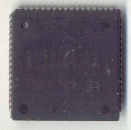
Intel 80286-12 - 1982 Though you can't read it very well, this is an old 286, the curse of the PC's being until Windows 2000 and XP. The 286's segmented addressing modes were famously described as "brain damaged" by Bill Gates and were the direct cause of the extended/expanded memory problems of '80s and '90s PCs. Architecture failings aside, the 286 was a very successful processor and this model in particular, the 12MHz, sold millions. In most 286 systems sold in Europe, however, the CPU was an AMD model, Intel had cornered the shorter shipping distances of the North American market from their assembly plant in Costa Rica while AMD had to export from their production facilities the southern USA. This particular part has a story behind it, like most other examples in this virtual museum. Sometime in the late 80s, a businessman was given an AMD 386DX-40 (see below) to work at home with. He used this machine quite well until 2000, when he came to me asking if it could be upgraded so his children could do homework on the Internet. It was a design seldom used today, where the entire I/O interfacing was on a pair of bridged ISA slots leading to a single, very large, daughterboard which had two IDE, parallel and serial ports. In a socket on this daughterboard was its controller, this 286-12. The slower 286s (8, 10 and 12 MHz parts) were usually ones to avoid. Not because they were bad, they weren't. It's because if we're not at least looking at a 16 MHz part, we're cutting corners. The "go to" in those days, late 1980s, very early 1990s, was a 16 MHz 286, 1 MB RAM (usually SIPPs), and a 40 MB HDD from Miniscribe or Seagate. If we wanted to play games, a 256 kB VGA card. If we were word processing or spreadsheeting, a 64 kB EGA card. Deviations from that were rare and usually meant something was wrong somewhere. The 286 almost always sat next to a 287 socket for the FPU, and just as almost always, that socket was empty. In all my years of dealing with PCs, I never found a 287 in the wild. The highest speed grade Intel made the 286 with appears to have been 16 MHz, but AMD and Harris made 20 MHz (which compared very favourably to 386SX) and Harris made a 25 MHz 286 (which was extremely speedy!). This set the scene for things to come. A new CPU would be on a new platform, new chipset, new motherboards, new technologies, all of which would together not be as aggressive as the top end of the older platform. The fastest 286s overlapped the slower (introductory) 386s and didn't cost the earth, so good video, good HDDs, and good motherboards could be used on the 286 machines. This pattern would be repeated again and again, the fastest 386s would be head and shoulders above the early 486s, the fastest 486s were far preferable to early Pentiums and so on. On this particular sample, a pin is broken off the PLCC package rendering this chip useless.
|
||||||||||||||||||||||||||||||||||||||||||||||||||||||||||||||||||||||||||||||||
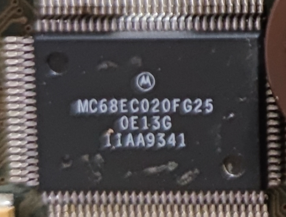 |
Motorola 68EC020 25 MHz - 1984 Motorola's 68000 series had been the main rival to Intel's x86 in the 1980s. 68000 had been limited by the number of pins on a cost-effective DIP (dual-inline package) being 64, and 64 was problematic. So 68000 had limited its data bus to 16 pins and address bus to 24 pins. It then could get away with just a 16 bit ALU, even though it described a 32 bit architecture: It took two memory bus cycles to read just one 32 bit word, so two ALU operations to process them wasn't a problem, the ALU wasn't the limiting factor. By the mid-1980s, a 24 bit address bus and a maximum of 16 MB of address was highly limiting for a processor which intensively used memory-mapped I/O, and 16 bits of data bus just wasn't fast enough. Motorola then began work on 68020, a "super-chip", fully 32 bits, 32 bits of address, 32 bits of data, 32 bits of ALU. Motorola designed it for a 169 pin pin-grid array package, which had become available, but ultimately only ended up using 114 pins. Another big change in 68020 was its move from NMOS to CMOS. CMOS was seen as bad, as it needed two transistors for a single gate, but Motorola felt CMOS' lower power use and faster switching would be beneficial. On announcement in 1984, this was breathlessly covered in the media and partners were clamouring for supply of this $487 (approx $1,200 in 2022) wonder-chip. Motorola had none. They could give samples, but volume production was not present. Their MOS-8 plant, had the latest CHMOS process licensed from Intel, but it had a yield of exactly zero. Every wafer which went through front end of line (photoresist, etching, etc.) and back end of line (metal layers, sealing, etc.) produced not a single working 68020. Not one. Management found that MOS-8 had been turned from a production facility into an R&D playground with non-standard equipment, no process standards, no production levels, not a thing indicating it was meant to be making the finest silicon on the planet. In one famous moment, Bill Walker (who had taken over MOS-8 with the task of rescuing it) discovered a Genius silicide machine didn't work in the slightest. He went to meet with Genius' CEO, who gave him the run around, resulting in Walker slamming his hands on the CEO's desk, demanding it is fixed "now, today" and breaking his watch strap. Genius later sent Walker a new watch strap. Walker had MOS-8 running properly by late 1985 and had it also making the new 68881 floating point unit. This chip was likely built in MOS-8, and has a date code of week 41, 1993. It is the 68EC020 model, which trims the address bus down to 24 bits. It retained the direct-mapped 256 byte instruction cache (it had no data cache) of the full '020, and other than the pins not being connected, was the same as any other 68020. 68020 could sustain a one in three instruction throughput, so attained around 8.3 VAX MIPS (as measured in Dhrystone) at 25 MHz. This one spent its life running at 28 MHz due to a quirk in its host system: The Commodore Amiga 1200. The clock supplied to the A1200's trapdoor expansion port was 28 MHz, so it was simplest to just use that. This CPU was mounted on a Blizzard 1220/4 CPU replacement and RAM expansion for the Amiga 1200. As 68020 was so late to market, thanks to the issues at MOS-8, 68030 was soon to replace it. 68020 remained a lower-end model for years, and enabled Motorola to keep prices on 68030 higher than they'd otherwise be. Its probably most famous use, other than the Commodore Amiga 1200, was in the ferociously expensive Macintosh II. Mac II had its own problems, mainly in that its OS misued address space, using the upper 8 bits of a 24 bit address to store data. This lack of "32 bit clean" meant it had to include a custom memory mapping unit to translate 32 bit hardware addresses to the 24 bit addresses the Mac OS expected! As the Mac II was cost reduced and matured, Apple raised its price by 20%, just because.
|
||||||||||||||||||||||||||||||||||||||||||||||||||||||||||||||||||||||||||||||||
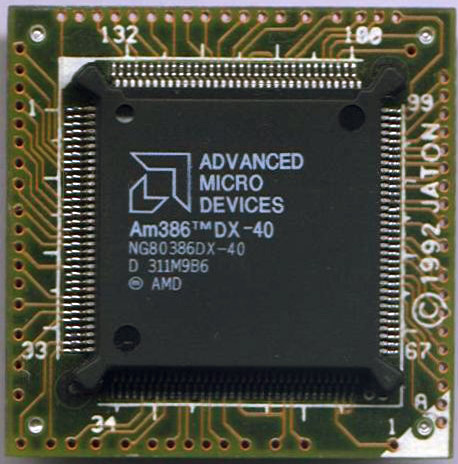 |
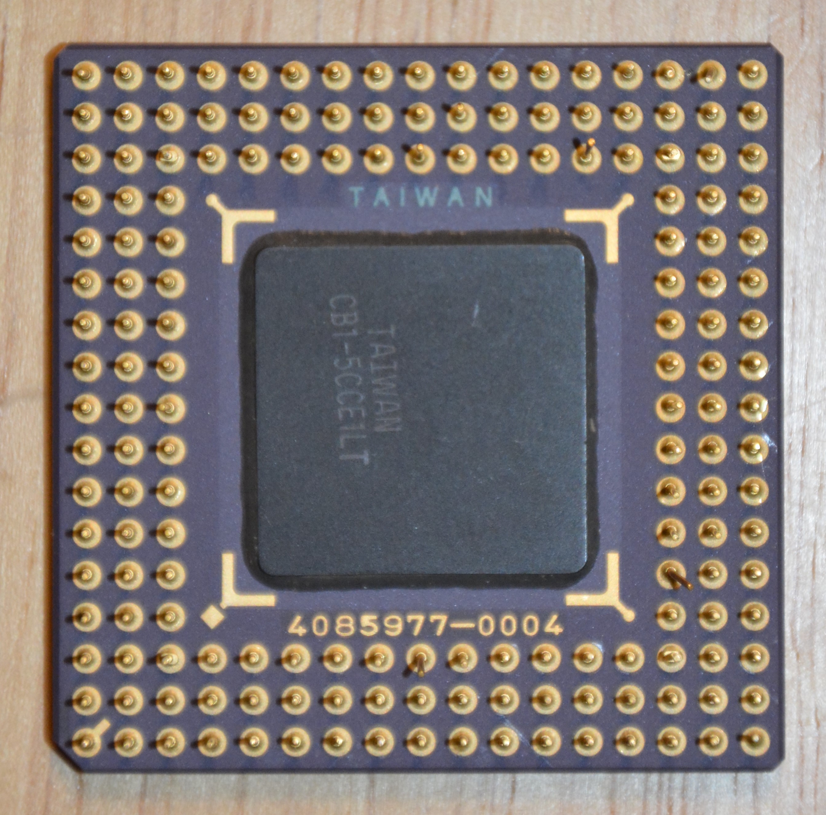
AMD Am386DX40 - 1991 Intel had tried to prevent AMD from producing chips with the name "286" and "386" with a lengthy lawsuit. The courts finally ruled that numbers could not be trademarked; This is why Pentium was not called P5 or 586, but was given a name so that it could be trademarked. AMD was forbidden via injunction from producing or selling 386s until the legal shenanigans were settled. At the time it was a massive victory for Intel, they had successfully delayed their competitor to market by years, even as the case was quietly settled out of court. Such legal stalling tactics are, and have always been, very common. Sidenote: Intel's 386SX (and AMD's) was not a "286 with 386 instructions", it was a real 386 with the data bus limited to 16 bits and its internal caches disabled. This allowed OEMs to use already qualified 286 motherboard designs and 30 pin SIMMs didn't need to be in pairs. Performance was severely impacted. Historically, the 386 made the PC platform what it is today. IBM had long had manufacturing rights to the 8088, 80186 and 80286, further they had mandated second-sourcing agreements, which meant that they could shop around for whoever was making the cheaper processors. With Intel seeking to prevent AMD from marketing 386s and the chip being very expensive, IBM didn't believe it the right time to release a 386 based machine. They were partly right. Nobody was to use the 32 bit modes of the 386 for almost ten years (the 386 debuted in 1986) and faster 286s could almost keep up with the slowest 386s. AMD, for their part, won the court battle and were finally allowed to start marketing their own 386s in 1991 after being held back for five years by Intel's legal blackmail. It was Compaq who broke IBM's deadlock on 286-only PCs. With a clean reverse-engineered BIOS (some say with substantial assistance from Intel) and a 386 machine, they opened the door to legitimate PC clones and heavy competition in the PC market. IBM lost their grip overnight, though machines were still branded 'IBM-Compatible' until the late '90s largely to hide the fact that they weren't. AMD's 386DX40 was a legend, those building computers at the time will be smiling, nodding and basking in the nostalgia. The introduction of a new platform tends to be a bit of a rough ride, early 486 motherboards were less than reliable and the processors themselves got remarkably hot to the point where many would fit small fans to them. Many prefered the older 386 platform which used reliable, proven motherboards from the likes of Soyo or DFI but even these couldn't deny the performance of even a 20MHz 486SX. The scarily expensive 25MHz 486s were faster still. Imagine Intel's chagrin when AMD produced the 386DX40, a processor capable of matching the FOUR TIMES as expensive 486SX20 bit for bit. To say that AMD's processor sold was rather like saying that water was wet. 486 was not to put enough distance between itself and AMD's DX40 until the 486 hit 66MHz with the DX/66. Where Intel's 486s had on chip caches, pipelined ALUs and faster MMUs to make it roughly double the 386 on a for-clock basis, Intel initially had difficulty reaching the 33MHz bin which would put it 'safe' beyond the capabilities of any 386. This meant that the 20MHz and 25MHz parts were able to be challenged, matched and, due to the finely tuned mature motherboards of the 386, even exceeded by AMD's 40MHz 386. While the 486 did have internal cache, it also had much slower access to RAM thanks to the 20/25 MHz system bus. AMD's 40 MHz system bus meant the cacheless 386 could keep up with and even exceed the 486s. The Am386DX40 probably took the PC platform to more people than any other single component and, in our view, is the greatest x86 CPU ever made. From 1991 to 1995, four long years, the Am386DX40 with 8 MB RAM, probably a 200 MB hard drive, was an excellent introduction to the PC. The big RAM quantity would help keep everything speedy. A small system builder near me (now sadly out of business due to some stupid decisions by the retired owner's son[1]) was selling very small slimline AMD 386DX40 systems with 16MB of memory and a 540MB hard disk even when the 486DX2/66 was the in-thing and he even put Windows95 on some of them (this was unwise). The 486DX2/66s were fast, very fast, but also very expensive. Most came only with 8MB of memory and perhaps a 340MB hard disk so in actual use a 386DX40 with 16MB of memory, still cheaper, could actually be the faster system! This particular chip was made in week 11 of 1993 (first three numbers of the line "D 311M9B6") and is mask nine, stepping B6. Note how the chip has no (C) mark, instead just the (M) mark. This is because the processor was made under patent license from Intel but partly designed and implemented by AMD. Also notice the odd packaging, the PLCC package mounted on a small PCB. The PCB was a socket pin adapter[2], able to mate the SMT-intended processor into a common socketed motherboard. [1]When you're known for your excellent service, your supporting a built and sold system FOR LIFE, your knowledgable staff and your general high quality, what do you do? Turn into a brand-name oriented shop which gives no support after the first year and refuses to stock AMD because "someone said they're unreliable". Then you wonder why business goes down the toilet and independent techs, like me, refuse to deal with you and explain to your father on the phone that the reason why is because you're a complete idiot.</rant> [2]Anyone with an actual ceramic Am386DXL40 is invited to submit it.
|
||||||||||||||||||||||||||||||||||||||||||||||||||||||||||||||||||||||||||||||||
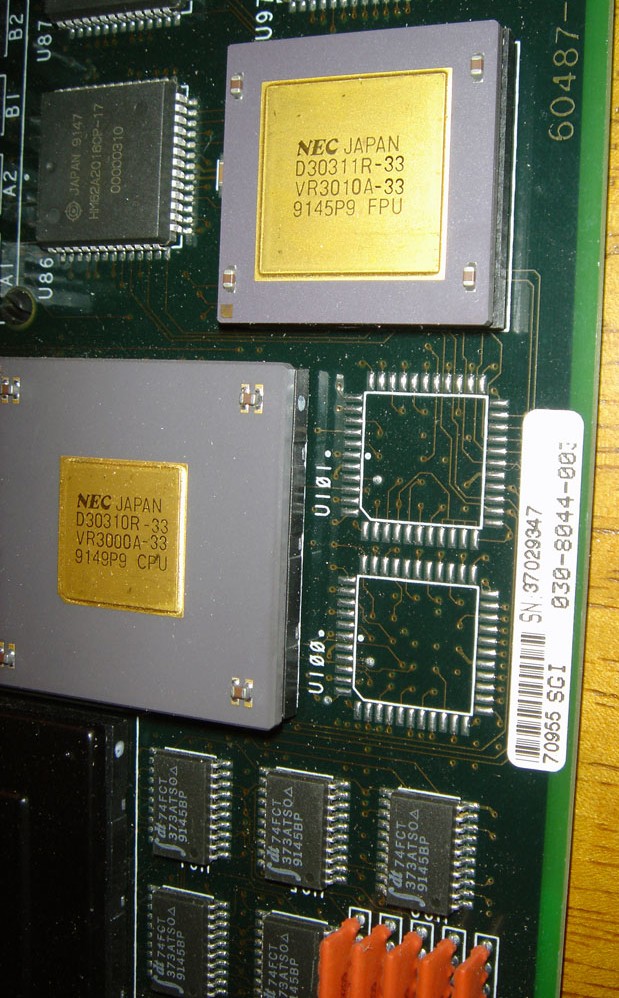 |
MIPS R3000A (MIPS R3000A) - 1991 On the right, the gold-coloured PGA packages, are NEC manufactured MIPS R3000 CPU chips. The larger one is the R3000A CPU, the smaller is the R3010 FPU, both clocked to 33 MHz. These implemented the MIPS III instruction set. The R3000A was a minor revision to reduce power use and enable a 40 MHz clock. The R3000A is also used as the CPU of the Playstation and as a secondary processor in the Playstation2. MIPS began as a project to make extremely highly clocked CPUs using very deep pipelines, rather like the much later Pentium4. To do this, complex instructions had to be removed as they took more than one clock cycle in an ALU, so the processor required interlocks to indicate when the pipeline was busy. MIPS was to remove interlocks by making EVERY operation take just one cycle, hence the name "Microprocessor without Interlocked Pipeline Stages". Each instruction on MIPS is fixed-length, each instruction word is 32 bits, the opcode (tells the CPU which operation to do) is 6 bits and it may have four 5 bit fields specifying registers to operate on. Extended formats were a 6 bit opcode and a 26 bit jump address (for a jump instruction, the CPU's "go to", used for branches) or the 6 bit opcode, a 16 bit data value and two 5 bit register identifiers. The actual commercial CPUs, such as this R3000A, did have hardware interlocks and did have multiply and divide (doing MUL or DIV was cheaper on bandwidth than being issued ADD or SUB over and over again, this plagued early PowerPC performance) and gained fame by powering these, SGI machines. The CPUs performance was really nothing special, but for their performance level, they were small, cheap and used very little power. By 1997, almost 50 million MIPS CPUs had been sold, finally taking the volume crown from the Motorola 68k series and in 2009, MIPS CPUs are still a high volume design, shipping more or less the same volume as x86. The competing British ARM design, however, out-ships absolutely everything else as much as four to one, it being the processor dominating the cellphone, PDA and embedded appliance (e.g. satnav, robotics) markets. MIPS R3000 has seen use in aerospace as the Mongoose-V, a radiation hardened version used in the New Horizons mission, the failed CONTOUR probe and its first use was in the Earth Observer 1 satellite. The Mongoose-V is manufactured by Synova and contains the R3010 on-die in a 256 pin QLCC package. In this SGI Indigo, the MIPS R3000A's largest competition was from the Amiga 3000, released two years earlier. This sported a 25 MHz Motorola 68030 but could not achieve the 30 VAX MIPS of the R3000A - the R3000A was a scalar processor, executing one instruction every clock, where the 68030 could peak at that, but many instructions took two or more clocks, resulting in the 25 MHz 68030 having a measured VAX MIPS performance of 10: Clock for clock the R3000 was three times faster. On a clock for clock basis, the R3000A's IPC (instructions per clock) was very nearly 1.0, the 68k series would not exceed this until the 1.2 of the 68040 (released in 1990, but extremely expensive and power hungry).
In this SGI, the QFP part labelled "HM62A2012CP-17" is one of the SRAMs used as L1 cache. The very presence of fast SRAM cache was necessary for the R3000A to be able to maintain its phenomenal performance. While complex processors such as the 68030 or 68040 could work straight from DRAM to near-maximum performance and needed only small L1 caches, the very simple instructions of RISC processors meant a lot of them were needed, which caused large amounts of bandwidth being used which would cripple any DRAM system, hence the requirement for expensive SRAM cache. The R3000 supports split I/D caches of 64-256 kB each.
Contributed by Evan |
||||||||||||||||||||||||||||||||||||||||||||||||||||||||||||||||||||||||||||||||
| [PROBABLY NEVER] |
UMC Green CPU - 1993 The UMC Green was available in the same common formats as other 486s and was made in "U5S" and "U5D" models. U5D was incredibly rare and had an x87 compatible FPU, which wasn't widely used or needed at the time. U5S was the one you were more likely to see. Of course Intel immediately threw lawyers at UMC, demanding that UMC give it all of the money in all of the world and UMC's president immediately kisses Intel CEO's dirty boot. UMC retaliated with an anti-trust suit. A settlement was reached, undisclosed, and both lawsuits were dropped. UMC agreed to keep out of the US market and focused its efforts on Europe instead. The early European Union a chillier welcome to foreign monopolists than they would find back home in the United States, so Intel did not pursue UMC there. UMC used only 8 kB L1 cache on the Green CPU, same as Intel and AMD, though Cyrix went higher with 16 kB caches. AMD in particular used a write-through cache which harmed performance. UMC put a lot of effort in optimising the microcode on what was essentially a hybrid of 80386 and 80486 technology levels (though, CPU-design architecturally, it was more similar to a souped up Motorola 68030) to reduce instruction latency. Being a pipelined CPU, having pipeline stalls (if a stage took more than one clock) meant downstream there was a pipeline bubble and potential work was not being done. UMC looked to minimise this by adding basic instruction scheduling (not proper out of order execution, there was no reorder buffer) to the decoders to avoid instructions getting hung up if it was at all possible to do so. Execution latencies were also much lower on UMC, complex instructions like divisions could be several times faster on UMC, meaning they got out of the way sooner, stopped using resources sooner, and so the CPU typically used less power. At 40 MHz, it ran like a 50 MHz Intel or a 66 MHz AMD. At around three quarters of the power to do so was icing on the cake for an excellent CPU. If you could find one (usually at smaller retailers in Germany or Britain, Intel threatened the bigger ones with "accidents" in their supply chain) it was your first choice. Due to the weird way Windows 98 Second Edition identified CPUs, it would identify a Green CPU as a Pentium MMX, which caused the OS to crash.
|
||||||||||||||||||||||||||||||||||||||||||||||||||||||||||||||||||||||||||||||||
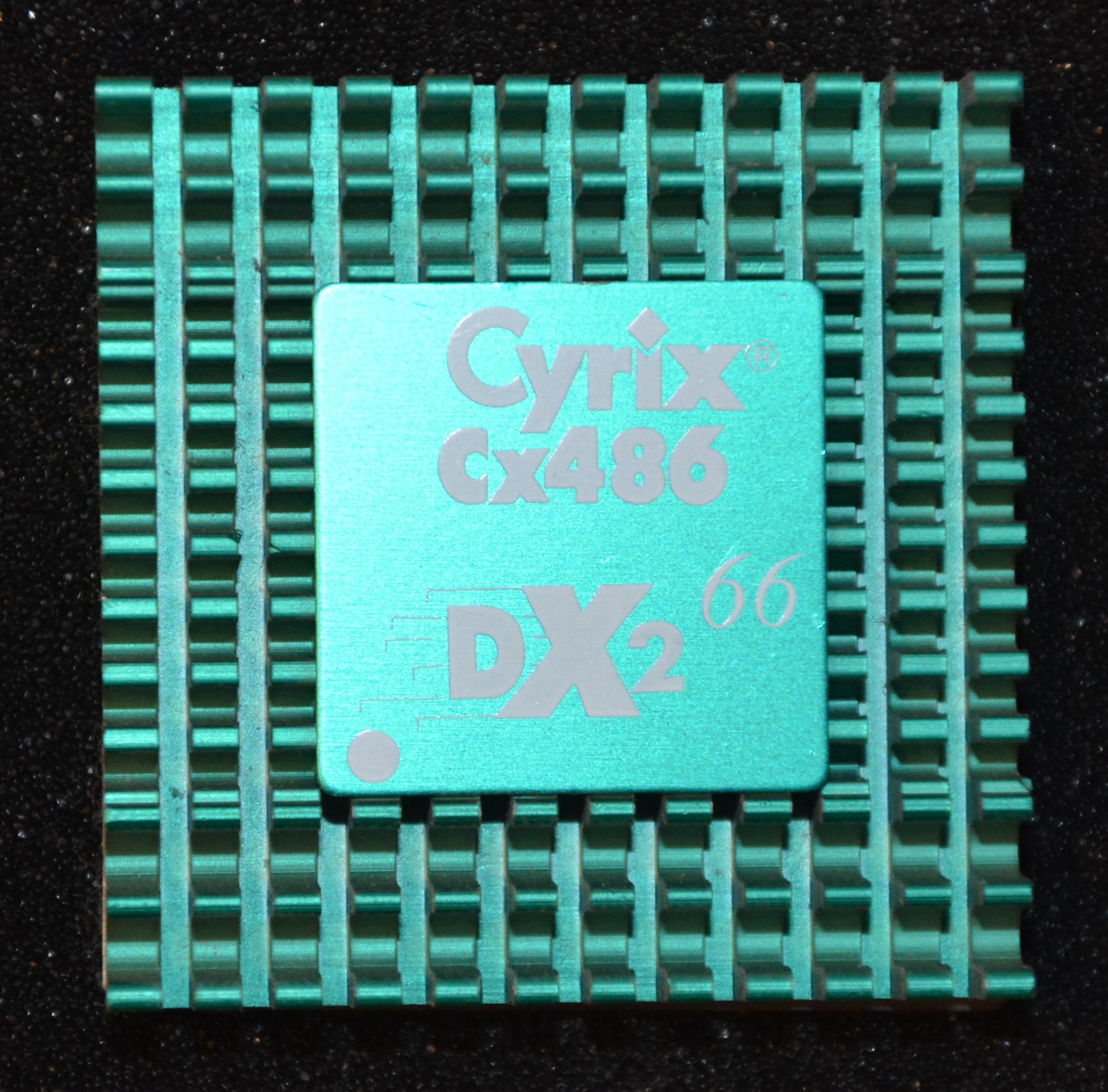 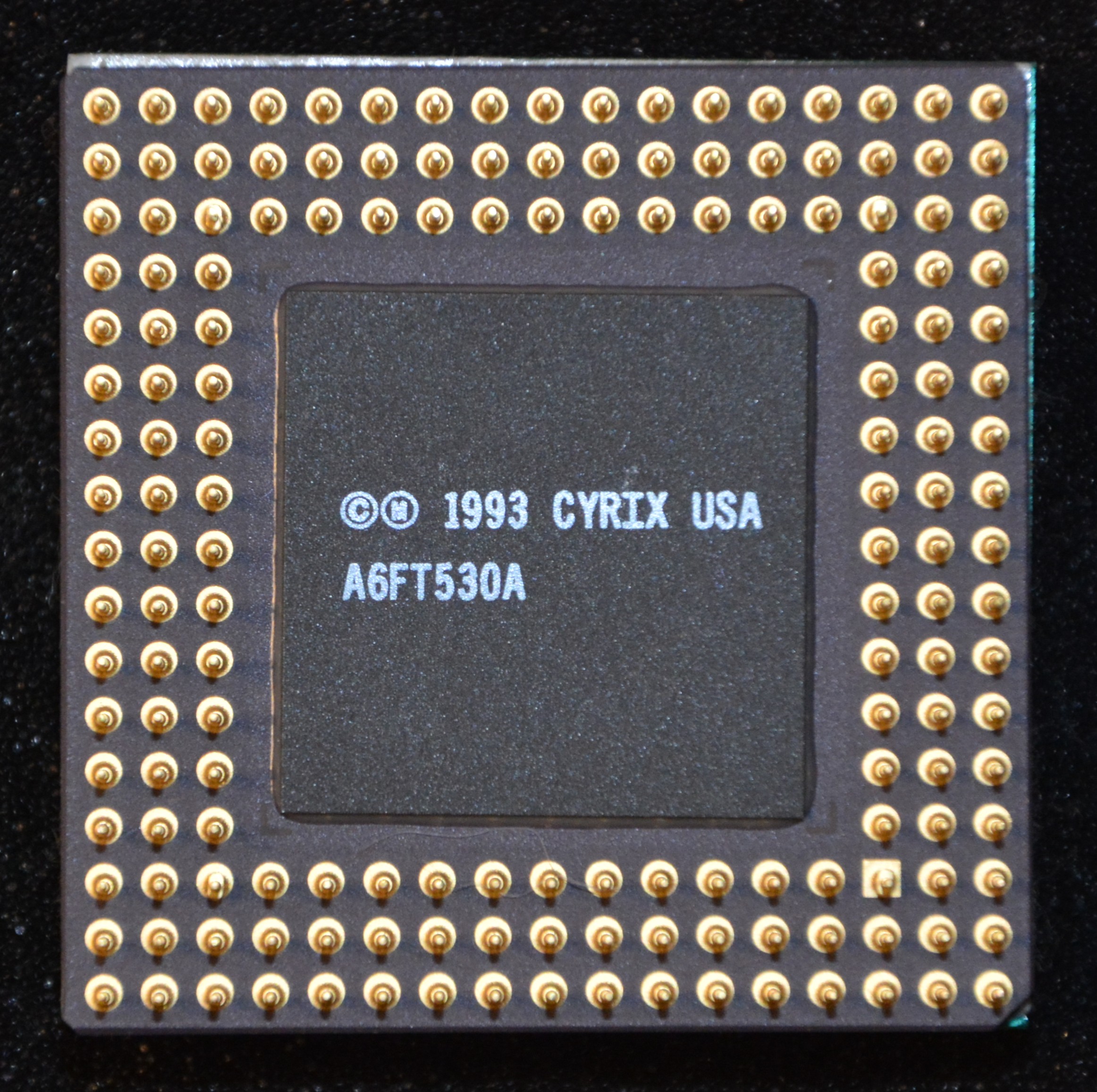 |
Cyrix 486DX2/66 - 1993 Cyrix's 486s hold a special place in many a PC technician's heart. They were typically a few percentage points slower than AMD or Intel, maybe a Cyrix 66 would run like an AMD 60. However, they would run on really janky motherboards. They were known to be very tolerant of shoddy signal integrity. L1 cache on the Cyrix Cx486DX was 8 kB and the whole chip ran from 5V initially, although 3.3/3.45V "split voltage" parts were available as the "Cx486DX2-V66". The earlier Cx486S, intended to compete with Intel's 486SX, had no FPU and only 2kB L1 cache: The FPU was a good 40% of the entire die on the 486DX versions, making a considerable cost-saving. Cyrix's units did, however, use write-back caches instead of the slower write-through caches. A write-through cache is smaller in silicon, but a write to memory stalls execution until the write has fully completed out to main memory. A write-back cache takes more logic to manage it, but the write only has to hit the cache and the CPU can continue working. Cache design was one of Cyrix's strengths and Cyrix chips usually ran their caches that little better than everyone else. The low-end Cx486S used a 2 kB write-back cache and also trimmed out the FPU. The DX2/66, as seen here, was the mainstream part. Cyrix did not make a 60 MHz version, and the 50 MHz version was hobbled on a 25 MHz bus. Only extremely bad motherboards would be happier at 25 MHz than the standard 33 MHz. From introduction in 1993 well to the middle of 1998, a Cyrix 486DX2/66 remained a reasonable processor, though slow toward the end of its useful life. Cyrix was, and would always be, fabless, so had fabs belonging to IBM, SGS-Thomson (ST) and Texas Instruments manufacture them. Part of the deal was that the manufacturers could sell some stock under their own name. Cyrix's processors ran better power management (i.e. they actually had some at all) than both AMD and Intel, so typically ran cooler and needed less power to do so. One of the rarer Cyrix 486s was the Cx486DX2-V80, which ran with a lower voltage, and with a 40 MHz bus to make an 80 MHz core clock from introduction in late 1994. They were surprisingly fast, even fast enough to run Windows 98, handle light Internet duties and play MP3s in 1999, but they were hellishly dated by then. Just playing an MP3 in Winamp was over 90% CPU utilisation on a 66 MHz 486 of anyone's manufacture. The code on the back is a manufacturing code. "A6FT530A" decodes as follows: A - Manufacturer (Unknown) 6 - Process (650 nm) F - Foundry (Unknown) T - Mask Revision 5 - Year (1995) 30 - Week (Week 30) A - Die lot code Manufacturers were G for IBM, F for Texas Instruments, so A was likely SGS Thomson (now ST Micro). Process is set per-manufacturer, so SGS process 6 is likely 650 nm. The foundry, in this case F, is again not well documented for SGS - possibly "France"? IBM used the first letter of the foundry location, which was one of Burlington, Corbeil, Fishkill or Bromont. In 1993, Intel slapped Cyrix with a massive patent-infringement lawsuit, intended to delay Cyrix in the marketplace. Cyrix responded, as UMC did before, with an anti-trust complaint. The courts found Cyrix had indeed reverse-engineered Intel's products, but the design was Cyrix's own and, on the eve of a Cyrix victory, Intel dropped the suit. Intel then paid Cyrix $12 million USD to drop the anti-trust suit. The damage was pretty hefty to Intel, as the court had found Texas Instruments, SGS-Thomson, and IBM were also validly licensed to manufacture and sell Cyrix CPUs using licenses they already had from Intel and that Cyrix was entitled to license its own design independently of Intel.
|
||||||||||||||||||||||||||||||||||||||||||||||||||||||||||||||||||||||||||||||||
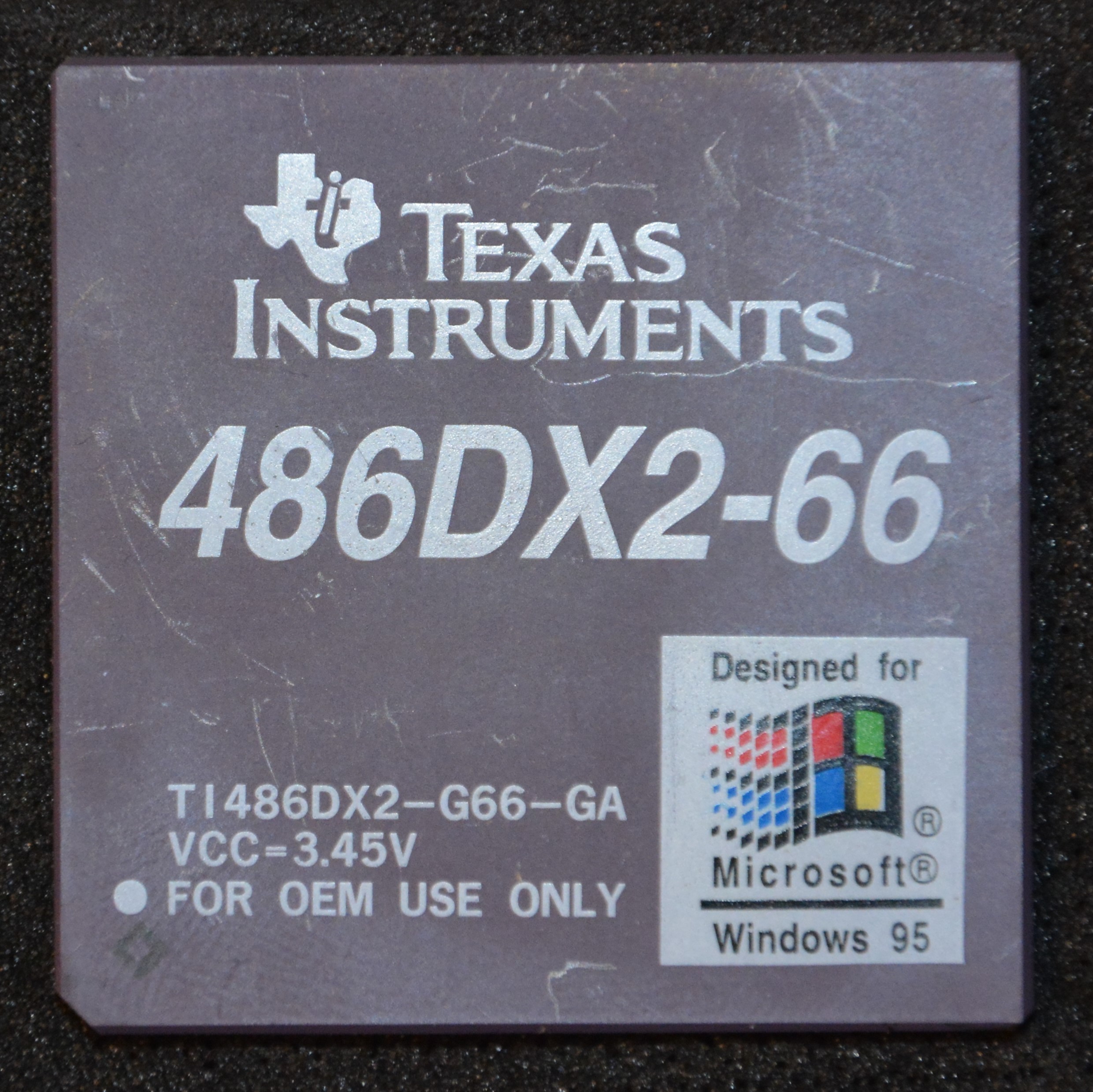  |
Texas Instruments 486DX2-66 - 1993
A Cyrix 486DX2-66 marketed by TI. Cyrix licensed out the design and allowed its partners (Cyrix itself was fabless) to sell some under their own names. Cyrix took retail sales, IBM, SGS-Thomson and TI sold their chips to OEM channels only. It was available with the Windows 3 style logo on it or the Windows 95 style logo on it. Texas Instruments produced these on its then-new 650 nm manufacturing process, down from the 800 nm earlier 486s were made on. This, in 1993, allowed a lower 3.45V operating voltage and peak power below five watts. TI would scale the DX2 from 66MHz, through the sometimes-iffy 80 MHz (due to a 40 MHz bus, which poor motherboards would not handle, and these guys tended to get put in poor motherboards) to a very quick 100 MHz with a 33 MHz bus cleanly multiplied 3x. Faster TI chips than 66 MHz were very rare: I never saw one in the wild, of the hundreds of CPUs which passed through in the late 1990s and early 2000s. By the time 66 and 80 MHz parts were around, Cyrix was pushing most of its output via IBM's manufacturing. They generally performed well, on par with an Intel or AMD 486DX2-66 or a little slower, due to Cyrix having to reverse engineer the microcode. The trouble is that they were too cheap for their own good. They'd go in extremely low cost motherboards, often with a very low amount of (or none, or even fake) L2 cache, hardly ever in a quality OPTI or ULI motherboard. They'd then be paired with a low amount of RAM (4 MB or 8 MB), slow hard disks, and you've got 1995's $999 cheap PC. So many corners cut that things suffered, a tale we see again and again. The CPU was chosen because it was lower cost, but then because the entire system is going for low cost, it's poor across the board. All this gave Cyrix CPUs a bad reputation, entirely undeserved, and they were well loved among independent system builders. So long as a quality motherboard, fast hard drive, and enough RAM (16 MB) were fitted, a Cyrix 486 made a saving of around $150-200, ran cooler and was unnoticably slower. It was sometimes said that a 66 MHz Cyrix ran like a 60 MHz Intel, but it was usually even closer than that: Perhaps 5%.
|
||||||||||||||||||||||||||||||||||||||||||||||||||||||||||||||||||||||||||||||||
 |
Cyrix 486 DX4/100 - 1995 A Cyrix 486 DX4/100 was a lot of things. Fast, cheap and late are among them. Cyrix had always made CPUs not by a licensing agreement, but by meticulous clean-room reverse engineering. Eventually Intel started to wave the patent stick and Cyrix fought back. On the verge of a Cyrix victory (which would have severely harmed Intel), a cross-licensing deal was worked out and the two parties settled. Many attribute the beginning of Cyrix's decline here, their failure to push the litigous advantage they had, which could have gained a much greater advantage for Cyrix than a mere cross-licensing deal. Back in 1995, when this CPU was new, the home PC (being sold as "multimedia") was starting its boom which would lead to the rise of the Internet. Intel's Pentiums were frighteningly expensive, so many prefered the 486s instead. 486s from all vendors still sold briskly even to the early part of 1997, but AMD and Cyrix had a sort of unwritten policy to sell their parts at the same price as Intel's one below. A DX4/100 from Cyrix or AMD would cost about the same as Intel's 66 or 80. As the chips themselves performed within a hair of each other, it took some very creative marketing from Intel - They usually spreaded FUD about how AMD and Cyrix were incompatible or not reliable. Utter bullshit, but it detered some buyers. Sure, it wasn't as fast as a Pentium but with 8 or 16 MB of memory (rarely 4 MB) they made a capable Windows 95 machine. Cyrix's DX4/100 was rated to a 33 MHz bus, a 3.0x multiplier and a 3.45V supply. It was actually more commonly used on 25 MHz motherboards with a 4.0x multiplier. Cyrix sold largely to upgraders, who valued Cyrix's compatibility, low prices and their ability to work, more or less, with very creaky motherboards. Where an Intel 486 DX4/100 wouldn't even boot, Cyrix's models would usually run with just a few stumbles. Cyrix's 486 DX CPUs consumed less power than Intel's models and featured much more advanced power management and a form of clock gating. While AMD and Intel made identical parts due to a licensing agreement (AMD had to adapt the design to its own manufacturing, and sometimes had to sacrifice things), Cyrix had to reverse engineer both the CPU architecture and its microcode. So while Cyrix made more compatible and lower power models, they were slightly slower. The 486 from Cyrix was also what is known as "fully static" meaning it could maintain its state without a clock signal, which Intel and AMD could not do, this enabled Cyrix to turn off the clock to parts of the die which weren't being used, saving even more power. Motorola's 68060 had also been manufactured this way. It wasn't purely a power saving move, however, nor even mainly one. A static design could run at a very wide range of clock frequencies without any sort of redesign or even anything at all, so Cyrix made one design and could sell it from 20 MHz all the way to 100 MHz. So long as power was still there, the clock could be stopped, execution would halt, power use would plummet to almost nothing, then the CPU could resume when the clock did. Cyrix were liberal with their licenses, entering into deals with IBM, Texas Instruments and SGS-Thomson for use of their production facilities, in return Cyrix allowed the aforementioned partners to sell CPUs under their own names. IBM in particular sold a lot of Cyrix's later 6x86 offerings.
|
||||||||||||||||||||||||||||||||||||||||||||||||||||||||||||||||||||||||||||||||
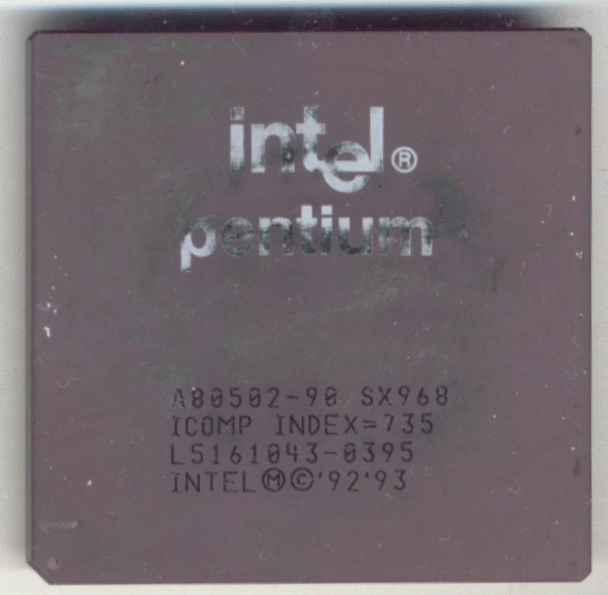 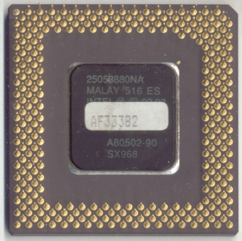 |
Intel Pentium 90 SX968 - 1995 This is when the Pentium became a viable alternative to the fast 486s. Before then, Pentiums had ran very hot, were buggy and quite unstable. They did not offer a justifiable (or often any) performance improvement over the 486 DX90/100/120s of the time. The first Pentiums were, believe it or not, released as samples as long ago as 1992, the 60 and 66MHz parts. The 50MHz sample is very rare and, strangely enough, all these early P5 parts sported 36bit physical addressing in the form of PAE. They were released to full manufacturing in early 1993, buggy, hot and far too immature. This was the P5 core with a maximum power of 16.0W at 66MHz, three times more than anything else. The pricing was also wince-inducing, costing around the same as an entire system made with a processor 60% as fast. Today, we're used to processors hitting 100 watts and more with huge coolers, but back then all we had were small heatsinks, rarely with little 40 mm fans sitting atop them, designed for the five watts of a fast 486. Sixteen watts was three times more than what was normal for the time! They were succeeded in 1994 by P54, the BiCMOS 800nm process refined to 500nm, the huge 294mm2 die reduced to 148mm2 and the huge 16W power requirement reduced to a mere 3.5W (for the 90MHz part, the 100 MHz was released at the same time). That was what I meant with "viable alternative". I'd be very surprised if any P60s or P66s survive to this day, but this P90 still runs just fine and was running an OpenBSD router until late in 2005. It was curious as to why Intel priced the 90 MHz part so high. Everyone was used to paying a huge premium for Intel's most powerful, but not for the second best, and the 90 MHz was the second best. By 1996, the Pentium to get was either the 90 or the 133. There was a 120, but this was very spendy for its performance level: The 60 MHz bus did it no favours. The Pentium got most of its performance from a superscalar pair of ALUs (the FPU was not superscalar but it was sort-of pipelined) which enabled it to double the speed of a 486 at the same clock on software specifically designed for it, or just luckily suited. Other enhancements were memory being twice as wide, 64 bits as opposed to 32 bits and more CPU cache. Pentium was not revolutionary, it was evolutionary. It was all the same design paradigms of the 486 before it, but each one enhanced, bettered, bigger, wider, faster. This one was manufactured in January (week 3) 1995 as demand for the Pentium (and the PC in general) took off as a result of Windows95. It was the C0 stepping, as the S-spec of SX968 tells us and it's the P54C core, which the part number of "A80502" tells us. A80501 was the original P5, and A80500 was used for the prototype P5s. The known P54C steppings are B1, B3, B5, C2, and E0. Usually steppings were used as a particular combination of manufacturing process version (processes were refined over time) and chip revision. All P5s had different voltage specs, so model 2 (P54C, the one here, P55C was model 4) had Std, VR, and VRE voltages. C2 raised VR's spec from B1/B3/B5 steppings' 3.135 - 3.465V to 3.135 - 3.600V, and changed VRE from 3.45 - 3.60V to 3.40 to 3.60V. Additionally, the B3 stepping fixed the problems B1 steppings had with power management. The HLT instruction and STPCLCK# line would cause the system to become "unresumable" in Intel's delicate phrasing. This was why no version of Windows9x supported using the HLT instruction in an idle-loop.
|
||||||||||||||||||||||||||||||||||||||||||||||||||||||||||||||||||||||||||||||||
|
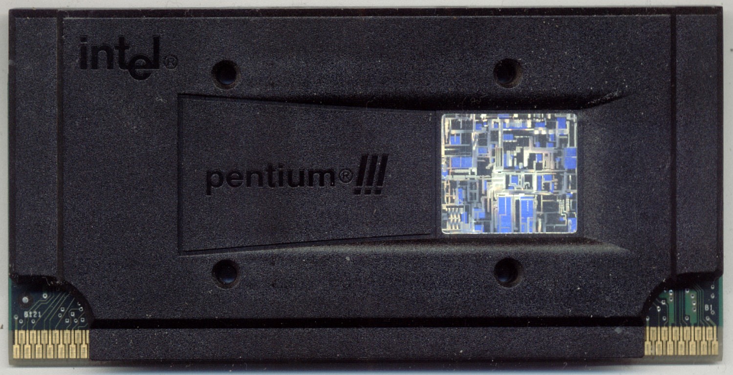
INTEL P6 Pentium had about taken standard CPU design as far as it would go and the rise of RISC super-microprocessors was seriously threatening Intel's dominance. The mid-1990s saw RISC CPUs many times faster than retroactively-named "CISC", a MIPS R3000A would run 30 million instructions per second from just 115,000 transistors, smaller than a 386. Intel knew the only thing keeping RISC processors from dominance was their price, which was caused by their reliance on expensive, fast, external SRAM caches. Intel also knew those expensive, fast, external SRAM caches could very easily be put on-die with how small a RISC CPU could be. The 1.2 million transistors of a 486 could allow a MIPS R3000A to have a 256 kB cache dropped next to it on the same die and that would be something scary. Preventing CISC CPUs reaching high performance levels was the low instructions per clock (IPC). While RISC CPUs would do around 1.0 instructions per clock, and an 80486 could actually sustain that on simple instructions, it had many complex instructions where it couldn't sustain an instruction each clock and usually ran around 0.4 IPC. 1.0 IPC was known as "scalar", while less than that was "subscalar". 1993's Pentium P5 was a superscalar CPU, it had two ALUs side by side and distinct address generation units, freeing up the ALUs from having to do memory address calculations. In most program code it reached 1.2 to 1.8 IPC. The performance leap from a fast 486 to a Pentium was enormous, though real system performance was held back by other components in most cases. What stopped Pentium from going to 2.0 IPC were pipeline stalls. The ALUs were fully pipelined, so ideally an instruction progressed from one pipeline stage to another every clock. Picture it like an assembly line, as that really is what it is. Occasionally a complex operation comes down the line and one of the stations takes more time than all the others, so the entire line has to stop. That's a pipeline stall. The other two problems facing the CPU were branches, where the instruction flow could go in different ways depending on what a currently-executing but not retired instruction did, and memory access. Memory latency had come down a lot with FPM and EDO technologies, and was around 30-40 nanoseconds. It would reach 20 ns a few years later, still during the life of the Pentium, then reach 10 ns and never again improve. While waiting for RAM, the CPU was plain idle, so it was important to have a large, well designed, CPU cache with a high hitrate. Pentium used two level 1 caches (L1$) of 8 kB each, one for code, one for instructions. It also use level 2 cache, motherboard mounted, on the CPU's front side bus, usually 128-512 kB, and made of fast SRAM. It wasn't any higher bandwidth than regular RAM (in fact was usually lower) but had a much lower latency, 1-2 nanoseconds. P6 took all the problems of Pentium, everything that challenged its performance, as its design statement. On Pentium, an instruction was microcoded, complex or simple. Microcoded instructions went to the microcode engine, which then took over the CPU until it had finished. Complex instructions could only go in pipeline U and simple instructions went to the U or V ALUs. To execute in pipeline V at all, a simple instruction had to be "paired" with another simple instruction in pipeline U, pipeline U would take its member of the pair in one clock, pipeline V would take its member in the next clock. On P6, this method of dispatching was completely binned. P6 instead decoded all instructions to "micro-operations" or "micro-ops" (μops). The IA32 ISA was complex and P6's decoder simplified it. The instruction fetch unit (which handled fetching from the bus interface, so RAM or L2$) or the instruction cache could supply two instructions per clock to the Instruction Decoder. Simple instructions went to one of the two simple decoders, and came out as one μop. Complex instructions had a single complex decoder, which could reduce them to one, two, three, or even four μops. Finally, really complex instructions were decoded by the microcode engine (and many of them partially executed there). This cluster of two simple decoders and one complex decoder could issue four μops per clock to the register renamer and reorder buffer. In practise, this took in two instructions per clock and emitted four (maximum) μops. The next stop of a μop was in the register alias table, where register renaming happened. x86 had eight general purpose registers and an eight-deep FPU stack, but architecturally the P6 had around 40 registers, which were assigned ("renamed") to instructions and data as needed. This register alias table then pushed the μops to the Reorder Buffer (ROB), which had 40 entries. The ROB was a really cool feature of P6. To combat pipeline stalls, P6 could do out of order execution, where instructions (so long as they had no dependencies) could execute as soon as something to execute them on became available. On Pentium, a long-running instruction held up everything behind it, even if the other execution pipeline was ready to accept more work. On P6, instructions could carry on being issued to the other pipelines. The "Reservation Station" fed these pipelines, including a memory interface unit which could handle load and store instructions itself, and the FPU, which was now also pipelined. In P6, the pipelines were made much longer. Pentium's five stage pipeline became 14 stages: Simpler stages could get their work done more quickly, as they had less of it to do, so the CPU clock could be much higher. Both ALU pipelines remained, both AGU pipelines remained. The ALU pipelines were now more symmetrical and each could handle (almost) any μop. P6 didn't have more execution hardware available to it than P5 did, but it did have the ability to keep them fed far, far better. A final area to discuss is branch prediction. On P5, a branch target buffer tracked the last few hundred branches and, if it was found to be identical to a previous branch, the branch was predicted. It was 256 entry and four way set associative. P6 bumped this to 512 entry and eight way set associative, but didn't otherwise improve it. It was bigger, but not smarter, and for a machine as deep as P6, that wasn't actually good enough. P6's basic architecture was not changed until Banias (Pentium-M) which reduced pipeline depth to 10 and so reduced the impact of mispredicted branches. P6 was introduced as Pentium Pro in 1995, reached the desktop as Pentium II in 1997, which had a minor revision in 1999 as Pentium III. 1999 had three Pentium III variants released, the original Katmai, the hugely improved Coppermine, and the enormous Cascades, which had 2 MB L2 cache on die, next to an otherwise unchanged Coppermine core. P6's last outing without major microarchitectural changes was as Tualatin in 2001, but this was not the end of the P6 story. A large microarchitectural rework of P6 became Banias, which formed the basis of the very first "Core" line of processors, as well as "Pentium-M". |
|||||||||||||||||||||||||||||||||||||||||||||||||||||||||||||||||||||||||||||||||
  |
Intel PentiumII 266MHz - 1997 Of stepping code SL2HE, this is a Klamath cored 266MHz part released in May 1997. The Klamath ran rather warm and only made it as far as 300MHz before the .25 micron die shrink to Deschutes took over. This particular part, as can be seen by a close inspection of the image, has had the B21 trace isolated in order to modify the CPU to request a 100MHz FSB. As this sample is also unlocked, then it can be made to run at 250MHz or 300MHz, both of which are a massive jump in performance over 266MHz thanks to the 100MHz bus speed and lower multiplier. The core has had its nickel plating sanded flat (lapped) to facilitate better contact with the heatsink, which helped it to reach 300MHz when overclocked. On either side of the core, one can see two SRAM chips, the processor has four of these rated for 133MHz and 128kB each. They do work when overclocked to 150MHz and they are clocked at half of CPU core speed. The reverse of the SECC (single edge contact card) shows the L2 tag RAM in the centre and the other two L2 SRAMS on either side. Despite what certain inaccurate publications will tell you, the P6 core did not have internal L2 tag, nor did it have internal L2 cache (internal = on die) until the Mendocino and, later, the Coppermine. The Pentium Pro also did not have on-die L2 cache or tag so let's put this to rest, the L2 tag and SRAM was housed on the same ceramic substrate (it was an MCM, multi-chip module, like Intel's Core 2 Quads) as the P6 die but was a distinct die.
|
||||||||||||||||||||||||||||||||||||||||||||||||||||||||||||||||||||||||||||||||
  |
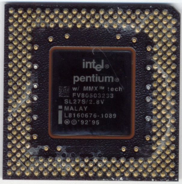
Intel Pentium 200 MMX SL27J - 1997 For release details, see the 233MHz part below. For this one, we'll have a look at why Intel disabled certain multipliers on the P55c (Pentium-MMX) series. For this, we need the codes on the bottom of the CPU package. The first on this one is "FV80503200". "FV" means organic substrate, "8050" is Pentium's model number, "3" is the code for the MMX Pentium, finally 200 is the rated clock frequency. It's nothing we don't already know. The kicker is the bottom code, "C7281004". The first letter is plant code - C for Costa Rica, L for Malaysia. (The 233 below is "L8160676") the next is year of manufacture, 7 being 1997. After that is the week of manufacture, week 28 in this case. Finally we have the FPO (testing lot) number at "1004". The next four after the hyphen are unimportant serial numbers. We were interested in the year and week. Before week 27, 1997, Pentium-MMX processors would recognise the 3x and 3.5x multipliers. For Pentium's 66MHz bus, this is 200MHz and 233MHz. After week 27, they would recognise their own mutiplier and no higher. This one would understand 1.5, 2, 2.5 and 3, but would not understand 3.5 - It could not run at 233MHz cleanly. Of course by running 75x3, we'd get 225MHz and often faster than the 66x3.5 because of the faster bus and L2 cache, but re-markers couldn't do that. Re-marking was a serious problem for Intel, unscrupulous retailers would polish off Intel's own markings, then re-mark the slower 166 and 200 parts and sell them as 233 parts! The chips didn't care, everything Intel was making would hit 233MHz, but Intel had to sell some of them as slower, cheaper parts so as not to cause a glut of the higher parts. Chips of part codes later than SL27H would usually always be multiplier restricted. Some rarer SL27K parts weren't limited but all past that were locked down.
|
||||||||||||||||||||||||||||||||||||||||||||||||||||||||||||||||||||||||||||||||
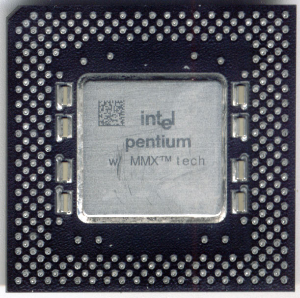  |
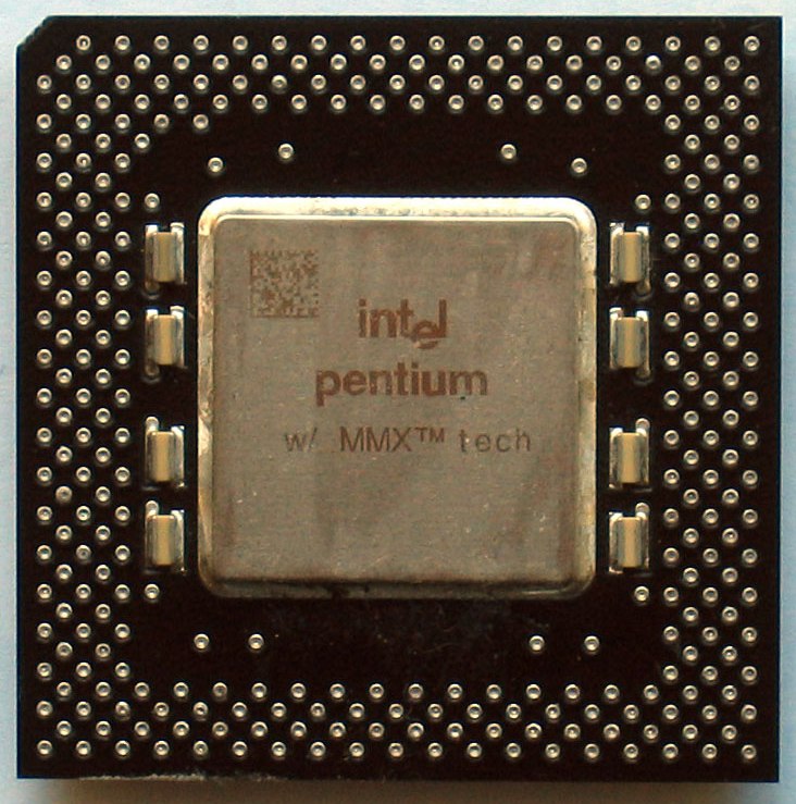
Intel Pentium 233 MMX SL27S - 1997 Amid a huge blaze of marketing in January 1997, Intel released their first MMX-equipped Pentiums, the 166, 200, a very rare 150MHz part and six months later a 233MHz part (after the 233MHz PentiumII). To believe the marketing, MMX was the best thing ever, but what really was it? Just after Pentium's production, Intel engineers wanted to add a SIMD (single instruction multiple data) extension to the x86 instruction set which would greatly accelerate anything that performs the same few operations on a great amount of data, such as most media tasks. Intel management, however, were a more conservative bunch and refused the request as it would require a new processor mode. They did allow a very limited subset of ALU-SIMD to be added, MMX. Not much actually used ALU-SIMD (media is FPU heavy) so MMX itself gave perhaps a 2% improvement on most code recompiled for it. The full SIMD extension would later come with Katmai as Katmai New Instructions (KNI) or its marketing/Internet friendly "Streaming SIMD Extensions", which of course "enhanced the online experience". Yep, the processor was claimed to make your Internet faster. What the new Pentium-MMX also had, however, was not quite so performance-agnostic. The original Pentium was originally made on the 800nm process node, but by the time of Pentium-MMX, Intel had a 350nm process available, meaning that less silicon was needed for the same parts, so yield was higher and manufacturing was cheaper. The P55c didn't just add MMX, it also doubled the size of the L1 cache from 2x 8kB to 2x 16kB which gave it a 5-10% boost on existing software across the board. P-MMX still could not keep up with the Cyrix 6x86L in office work environments and was very little faster than Pentium in media environments. It gained the inglorious distinction of the first ever Intel CPU to be defeated by a competitor: Cyrix's 6x86L-200 was faster than Pentium-MMX 200. The 1997 release of the Pentium-MMX was seen as too little and too late, it did not differentiate itself from Pentium, it was expensive and hyped up by Intel so much that consumers were expecting something better than a refresh of a five year old part. Part of the problem was that, at the 200 MHz grade (and certainly at the 233 MHz one), the 66 MHz bus speed just wasn't enough. AMD and Cyrix had already pushed 75 MHz bus speeds with success, and Cyrix was talking up an 83 MHz bus. The extreme bottleneck of the 66 MHz bus would be why Intel used it for its Celerons well into the 800 MHz range!
|
||||||||||||||||||||||||||||||||||||||||||||||||||||||||||||||||||||||||||||||||
  |
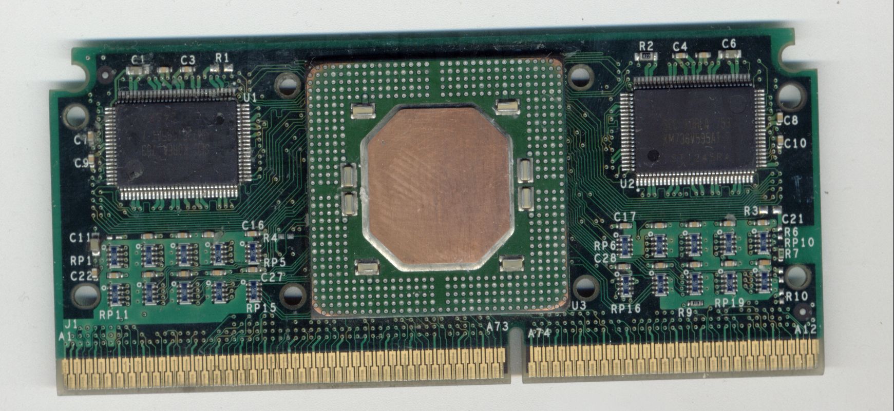
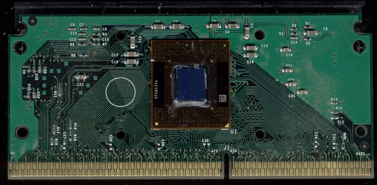
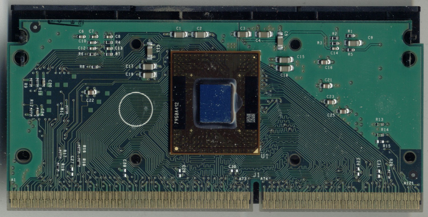
Intel Mobile Pentium II 233 - 1997 Intel's mobile "Tonga" Pentium II was really just Deschutes, the desktop Pentium II and it was pretty much identical but for form factor. The MMC-1 cartridge, seen here, packed the northbridge on the cartridge so that it was impossible to use cheaper VIA or SIS chipsets with the mobile Pentium II and for Intel, more sales. In this case, the well-regarded 440BX chipset.
|
||||||||||||||||||||||||||||||||||||||||||||||||||||||||||||||||||||||||||||||||
|
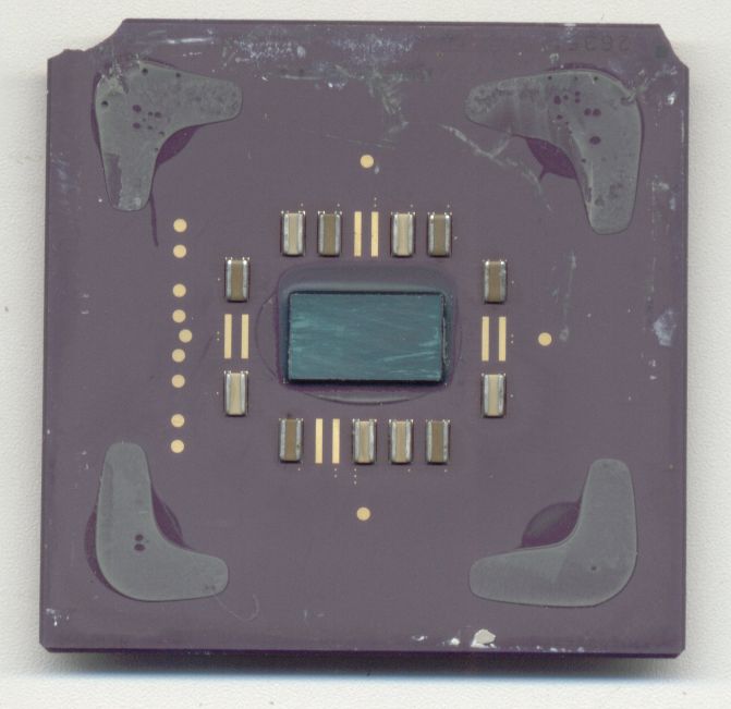
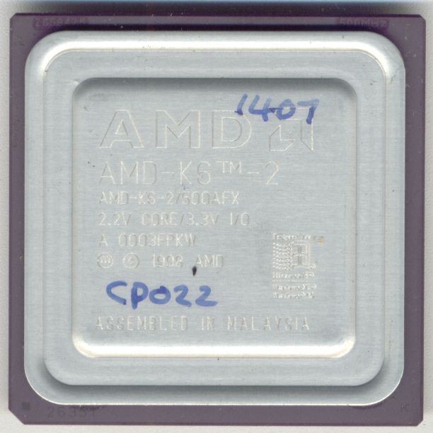
AMD K6 No discussion of the CPUs in the 1997-1999 timeframe can be complete without AMD's K6. AMD's previous K5 had been an adaptation of its powerful Am29000 RISC processor to run x86 code, since AMD was now making in-house CPU designs instead of licensing Intel's. So, AMD K5 decoded x86 instructions into "RISC86" instructions, which were basically AMD's 29K instruction set. The CPU was out of order, using a then-modern reorder buffer (ROB) and could issue four operations per clock to two ALUs, one FPU, oen branch unit, and one of two load/store units. It even had instruction queuing in "reservation stations" ahead of each functional unit (something Zen brought back with its non-scheduling queues!) K5 was a seriously powerful piece of kit, a 66 MHz model would easily match a 100 MHz Pentium, but it was a stop-gap architecture. Nobody in AMD seriously thought the whole RISC86 thing was in any way sustainable. Decoding instructions was a good and proper thing, but decoding them for an entire different CPU architecture was not, there were "front-end" things in it which didn't need to be there, for example. So AMD bought NexGen. NexGen's 6x86 was technologically on the same level as AMD's K5 but far more integrated and elegant than AMD's bodgy K5 had been. K5 was a good stop-gap, but still only a stop-gap. Nx6x86 had much more future to develop from. AMD stuck NexGen in its own building, was very hands-off with it, and told them to make a Socket 7 processor from the Nx6x86. Intel would not allow AMD onto the Slot-1 and later Socket 370 platform. K6, while having little architectural heritage from K5, was largely the same kind of processor. The same quad-issue instruction decoder (two instructions in per clock, four RISC86 operations out, though not the same "RISC86" as K5), a 24 entry scheduler able to issue six operations per clock, with no reservation stations. Back end execution resources were two ALUs, independent load and store units, a multimedia unit (did MMX on the K6) and a floating point unit. You did not want a K6 for a gaming machine. Games back then were heavy on floating point, since that was how geometries were rotated and scaled for render: GPUs couldn't do it (and nobody used the term "GPU"!) and AMD's FPU in the K6 was quite basic. It was pipelined, though with only two stages. If the first stage was busy for many clocks, the second stage sat idly doing nothing. If the second stage was busy for many clocks, the first stage also stalled. The FPU was lower latency on many instructions than anything else, but it had to be. FPU throughput, clock for clock, was about 80-90% of Pentium and around 30-40% of Pentium II. In anything that wasn't a game, however, K6 was easily Pentium II's peer. AMD boosted clocks massively in K6-2, and added "3DNow!" (a large extension to MMX) which hugely helped game performance, if it was used. DirectX 7 would use it, but the game itself also had to use it for full benefit (DX7 would do geometry transformation, setting it up for display, but not vertex translation, used for animation) K6-2 was financially very successful for AMD and bankrolled the development of K7. The final version of K6 was the K6-III, which added 256 kB L2 cache to the die, which was very significant in performance. Die-shrunk to 180 nm, as K6-2+ (128 kB L2 cache) and K6-III+, they represented quite worryingly high performance... But cost almost as much as a K7 to manufacture, so AMD didn't make too many of them. People who found a K6-III+ (or its cache-disabled K6-2+ variant) noted it would clock extremely high, presumably it was a backup plan to buy time of AMD's K7 launch went awry. To enable this, K6-III+ remapped the "2x" multiplier ID as "6x" (something the K6-2 had also done, but K6-2 would almost never reach 600 MHz). Using extremely well engineered motherboards (rare on AMD's Super Socket 7 platform), could overclock to around 800 MHz with the CPU being quite happy there. This would be achieved by setting front-side bus (FSB) to 133 MHz and the CPU multiplier to 2x (interpreted as 6x by the CPU), for 800 MHz. Most motherboards were extremely unhappy above 110 MHz FSB, very few would work at 112 MHz, and practically none would go to 133 MHz. To get it there, the enthusiast (with far too much time on his hands) would have to de-solder the motherboard mounted cache, which was practically never rated for 133 MHz operation, and replace it with faster SRAM able to run at 133 MHz or just plain disable the onboard cache. Many SiS530 chipset motherboards used the ICS9248AF PLL to generate clocks, which was able to cleanly clock 133 MHz FSB and 33 MHz PCI. Disabling (or replacing) the onboard cache on these would get you your 800 MHz K6-2+ or K6-III+. Just for completeness, the FIC PA-2013 motherboard was very popular in the day, it remains popular for retrocomputing due to its very large cache and good performance. Ensure you have revision 2.1 or above of this board, the earlier versions lack a discrete AGP voltage regulator and can actually burn out with GeForce 2 and Voodoo3 video cards. |
|||||||||||||||||||||||||||||||||||||||||||||||||||||||||||||||||||||||||||||||||
| No Image Yet |
Cyrix MII PR300 - 1998 The Cyrix MII has a special place in my heart as it was the CPU of my first ever fully self-built PC. Cyrix's designers were among the best in the industry, while AMD had always produced CPUs via a cross-licencing agreement with Intel, Cyrix had no such agreement and had to only licence the patents. Cyrix did exhaustive clean-room reverse engineering as well as its own design work. The 6x86 (which formed the basis of the 6x86L, 6x86MX, and MII) was Cyrix's greatest triumph but also its downfall. When the design project began in late 1993, almost all PC software was very heavy on ALU integer operations, so Cyrix focused efforts there and put in a floating point unit (FPU) to do FP operations, but didn't sacrifice ALU integer performance to make FP faster, nobody would benefit. When released, in mid-1995, the 6x86 was the fastest x86 processor on the planet. It was so fast that a 133 MHz 6x86 would usually perform about the same as a 166 MHz Intel Pentium, so Cyrix rated its CPUs with a "performance rating" - A 133 MHz 6x86 was "PR166". What Cyrix did not see, frankly nobody did, was the rise of FPU importance. The early "corridor games" like Doom and Doom II did some 3D processing but did it all in integer arithmetic, Doom used path-tracing (to come back some 30 years later!) to find intersections in 2D space. Doom was really 2D but with a 3D viewport, sometimes called "2.5D" because the vertical dimension is actually fake, the player can't go up or down, can't look up or down, and features can't be higher or lower. Hower, id Software was working on Quake, which was fully 3D. This couldn't be easily calculated using high performance integer calculations, it had to use floating point. CPUs of the day were very bad at floating point arithmetic. A 66 MHz Intel, AMD, or Cyrix 486 could easily top 60 million integer operations per second (MIPS, million instructions per second), but 2-5 million floating point operations per second (FLOPS). As we discussed earlier, FP wasn't something any PC software did much of but Quake had to do lots of it. Even AutoCAD, which was the poster-boy for FPU performance, used FP only where it had to. A quirk of Intel's Pentium FPU design came in next. To avoid wasting space on FP, when few people used it, it was broken up into an four-stage pipeline, being two execution stages, a rounding stage, and a write-out stage. Only very simple instructions like FMUL could execute in one clock per stage, so it stalled often. Because it shared the address generation, decoding, and dispatching with the two integer pipelines, Intel did not put much devotion to FP in the decoder, it could only output one FP instruction every four clocks, so the very fastest a 100 MHz Pentium could do FP was 25 MFLOPS... Which was, on average, five times faster than a 486 at the same clock. So while the Cyrix MII was 1.5x faster, clock for clock, than its previous 486 (and a solid generational improvement!), Pentium was around three times faster even than that. Quake ran far better on a Pentium than on a Cyrix. It wasn't even close. In the modern day, it'd be like putting Intel's E-cores up against AMD's X3Ds. Ordinarily this wouldn't matter, not that many people cared much about Quake... 3D games were the massively hyped and rapidly growing thing in the latter half of the 1990s. High performance 3D with 3D accelerators built into video cards (or even their own PCI devices!) relied on the host CPU being able to set geometries and triangles up fast enough, which was all highly FP intensive. A Cyrix (or AMD) CPU was absolutely not what you wanted. As the fastest growing part of the PC market was the home PC, and games were important for these, this meant Cyrix and AMD had little to sell at the higher side of the market. The 6x86 had one major redesign in its life which added MMX and increased L1 cache from 16 kB to 64 kB. It started on a 650 nm process (or .65 μm) and the last few were 180 nm running on the 100 MHz Super 7 platform, the MII PR433, which only ran at 300 MHz, the PR on that was very optimistic. By the time Cyrix had endured being bought by National Semiconductor (to be ran into the ground), the M3 project (M1 had been 6x86, then M2 was 6x86MX, later renamed to MII) was running far behind schedule, since NatSemi wanted Cyrix to make a full x86 system-on-chip, the MediaGX. This was a 5x86 from years before with NatSemi's Xpress peripheral devices (RAM controller, video output, audio) on-die. When NatSemi sold Cyrix to Via Technologies, then a big player, Via cancelled M3 entirely.
|
||||||||||||||||||||||||||||||||||||||||||||||||||||||||||||||||||||||||||||||||
| No Image Yet |
Intel Celeron 300MHz - 1998 The bastard offspring of Intel's price premium craze in the PentiumII days, this was the CPU that was, in June 1998, to take market share in the low end, where AMD and Cyrix were having their own party. The lack of L2 cache left the P6 core choked for data, the 66MHz FSB didn't help either. Coupled with the low end motherboards, this CPU's performance was dismal. Before we look at the original Celeron, this one, we need to understand the market conditions it was aiming for. Intel had just moved to the P6 core, as Pentium-II, which ran on a SECC cartridge with off-die L2 tag RAM and L2 cache, which ran at half core clock. This was expensive, 512 kB SRAM rated for 150-250 MHz was not cheap in 1998, even as Intel was manufacturing it itself. So, a 300 MHz Pentium-II was very fast, but also very expensive. Intel was unwilling to lower prices on it to offer slower variants, seemingly seeing the "Pentium-II" brand as a premium brand. Raining on the parade was Cyrix and AMD. With CPUs around a third of the price of the Pentium-II, they'd pushed Socket 7 to "Super 7", with 512 kB to 1024 kB motherboard cache (at bus speed, 100 MHz), running 100 MHz SDRAM, and hitting 70-90% of Pentium-II's performance. Intel had only Pentium-MMX to compete there, which ran on a 66 MHz bus, clocked no higher than 233 MHz, and was generally uncompetitive with AMD or Cyrix. Intel was being threatened by being both undercut and outperformed in around two thirds of the entire market: While Intel had volume, volume means nothing without an actual product to ship! So Intel both wanted a premium product and volume shipments. Something had to give. Celeron would be that product. A simple P6 core, no L2 cache, none at all, which helped bring price down to just a tiny bit over a similarly clocked AMD K6. Performance, however, was lousy. Usually, a lousy CPU had an excuse. It had a reason. Something caused it to be like it was. The AMD K5 was delayed by unforseen problems in development. The original Intel Pentium was just too transistor heavy for 80 micron BiCMOS. The VIA C3 was never intended to compete in the performance market. AMD's Bulldozer was saddled with 16 kB L1 data cache because of difficulties with high speed SRAM and the die layout. The Celeron had none of these excuses. It was actually designed to stink. It had no L2 cache whatsoever and performance was typically less than the elderly Pentium-MMX 233 it was meant to replace. AMD's K6 went unchallenged and gained popularity dramatically as a result They weren't all bad, since games of the time rarely needed much in the way of L2 cache and showed only a marginal drop in performance on the cache-less Covington. An overclocked Celeron with a Voodoo3 was a cheap, but powerful, Quake3 machine. It was just utterly awful at anything else! The 300 MHz cacheless Celeron would be outperformed by any half-way decent system with a Pentium-MMX at 200 MHz or so in anything which wasn't games... and even some games. This is the "Covington" core, which is absolutely nothing more than a very slightly tweaked Deschutes, and shares its overclockability, hitting 450MHz with only a modest heatsink. The CPU is partly lapped to facilitate a better heatsink fit, but didn't make it past 464MHz. The PentiumII 266 running at 300MHz still outperformed it substantially, such is the importance of L2 cache. The redesign of this CPU, to incorporate 128kB L2, was known as Celeron A or "Mendocino", the famous Celeron 300A being one example.
|
||||||||||||||||||||||||||||||||||||||||||||||||||||||||||||||||||||||||||||||||
   |
AMD K6-2 450AFX - 1999 The 450MHz and 500MHz K6-2s were everywhere in 1999 and 2000 after their release in February 1999. The 500MHz parts were hard to get hold of, it seemed everyone wanted one, but the 450 part was king of the price/performance curve. In a world where Intel was selling the 450MHz Pentium-II for £190 and the 500MHz Pentium-III for £280, the £54 that you could get a K6-2 450MHz for was an absolute steal. That in mind, the K6-2 would often run rings around the Pentiums in daily usage, as long as your daily usage wasn't games. You very much did not want a K6-2 for games. Back then, games were very FPU intensive (the GPU does this these days) as part of their lighting and geometry transformation workloads, and K6-2 plain did not have a powerful FPU. In something like Quake 3 Arena, A K6-2 450 would run around the same as a Pentium II 266. Ever since Cyrix had become the first x86 maker to claim the performance throne with the 6x86-200 in 1996, Intel had seemed weak. The Slot-1 platform was indeed performant, but it was 100% Intel-only and lacked that competitive drive. Intel took back its rightful crown in 1997, only to lose it months later to AMD's K6-233. It's important to remember that, in this era, gamimg performance was not as important as it was to become in the 2010s and onwards, we used PCs for work much more than play, so AMD's very powerful K6 series, even with thee gaming handicap, were still among the finest CPUs money could buy. AMD continued producing K6-2 450s for over two years, they were still common in 2001. By this time they were typically 2.2 volt and, sometimes, really K6-III chips which had defective L2 cache. Either way, they made excellent, and quite cheap, little machines for running Windows 2000 on. Once you'd found a motherboard you liked (usually a Gigabyte or FIC with the ALI Aladdin V chipset), they worked first time, every time, and went well with a few hundred MB of PC-100 SDRAM. This part was paired with the GA5-AX motherboard in the motherboards section and 192MB of PC100 SDRAM (three 64MB DIMMs), such a combination would have been quite formidable in 1998. In 1998 and 1999, the big seller everywhere was the K6-2. It was cheap, fast, and reliable. The K6-2 was pretty poorly named, it was the K6-3D, it had a SIMD instruction set known as '3DNow!' added; Much like SSE but a bit less flexible and a bit more streamlined. This made the K6-2 much faster in supporting games, a field where it had traditionally been quite poor. It was not, however, a new processor. Intel was to copy this misleading naming shenaniganry with the Pentum-III, which was nothing at all more than 'PentiumII-SSE' until Coppermine.
|
||||||||||||||||||||||||||||||||||||||||||||||||||||||||||||||||||||||||||||||||
 |
AMD K6-2 500AFX - 1999 These things sold like hotcakes in 1999 (after their release in August) to 2000. The psychological "half gigahertz" barrier could be broken by a Pentium III, fiendishly expensive and widely understood to be no better and little different to the aged Pentium II, or by a K6-2. The Pentium III was three to four times the price of the K6-2 and performed slightly worse in most tasks other than games. For many, that wasn't a compromise worth taking and the higher K6-2s were AMD's most successful product since the amazing little Am368DX40. There was also a K6-2 550 but these were always in short supply (which drove up the price and made them less attractive) and represented about as far as the K6-2 could go on a 250nm process. I never really saw a K6-2 550 which was happy at 550. Most K6-2s by this time were marked to 2.2V (some slower ones were 2.4V) and the 550s were rated at 2.3V, so overvolted out of the factory, and not happy about it either. You'd normally have to knock them down to around 525 (105 MHz bus) to make them stable. By the time AMD was shipping 550s, the 400 MHz K6-III was around the same price and very, very fast. Later, the quietly announced K6-2+ (with 128 kB of L2 cache onboard) appeared which was also quite scarily fast, but hard to find. The K6-2+ was later revision of the K6-III where a failure in part of the L2 cache could be walled off into a 128 kB chunk, disabling only half the cache.
|
||||||||||||||||||||||||||||||||||||||||||||||||||||||||||||||||||||||||||||||||
|
No image yet |
AMD K6-III 450 - 1999 Never actually came across one of these, but this area felt a bit bare without it. AMD's K6-III was one of the all-time greats of the industry. It was the undisputed, unchallenged king of business computing for 1999 and 2000, while Athlon was still a little too expensive for buying 50 of them to outfit an office and Durons were yet to take over. K6 was already a good performing core design, adding full speed L2 cache to it really helped it along and they routinely sold for less than £100. They were just under twice the price of the K6-2 500, about 25% faster, so didn't make sense compared to the K6-2 500, but compared to the Pentium-III, they were almost a complete no-brainer. A third of the price, faster in almost everything (other than games) and not on the very pricey Slot-1 platform: K6-IIIs used the same proven and mature Super 7 motherboards as the K6-2 did. They flew on the 512 kB L2 cache of a Gigabyte GA5-AX, and positively screamed along on the rarer 1 MB cache boards. Intel's competition at a similar price was the Socket 370 Celeron, 433 and 466 ratings. They were good for low-cost gaming, but for the money you were better off with a K6-III and a more powerful video card. K6-III would not be matched by any Celeron in business or productivity computing until it became discontinued. Oddly enough, a K6-III 450 was 5-20% faster than a Pentium II Xeon 450 with 512 kB L2 cache at Microsoft SQL Server 7.0 and held itself proud against the immensely expensive Pentium II Xeon 450 2 MB. With the same RAID-5 (hardware, on an Adaptec PCI SCSI-III controller) array, same 128 MB PC100 memory, the cheap little K6-III 450 ran around the same in a high end database server as a CPU fifteen times the cost! For those in the know, the K6-III was a frighteningly effective processor. Later, AMD moved the K6-III to a 180 nm (.18 micron) process and sold it at the same clocks as a low power K6-III+. They were nothing special, until you overclocked them. They'd hit 600 MHz. You'd up the FSB to about 110 MHz (the fastest most Super 7 boards could go, thanks to the onboard cache) and hope for 605 MHz, maybe with a 2.1V core voltage (they were rated to 2.0). If you didn't make it, you'd drop the multiplier to 5 and 550 MHz worked with nearly all of them. At this speed, they were keeping up with Durons. Fast Durons. K6-III was one of those parts which never really got around enough to be appreciated as much as it should have been. It was the performance leader for almost a year.
|
||||||||||||||||||||||||||||||||||||||||||||||||||||||||||||||||||||||||||||||||
 |
Intel PentiumIII 600E SL3H6 - 1999 A micro-BGA package slapped onto a quick slot adapter and sold mostly as an upgrade for existing Slot-1 owners from October 1999. They rapidly became popular with OEMs who could use their already qualified Slot-1 designs with the new Pentium IIIE processor. The E denotes the presence of a Coppermine with onboard L2 cache, the 133MHz one was EB, the B meaning the 133MHz bus. Confused yet? P3 went through no less than THREE different CPU cores or, indeed, five if you include the Xeon derivatives. To make it even more confusing, I'm told that some slower mobile P3s were actually the PentiumII Dixon and didn't support SSE and that some mobile PentiumII parts were actually P3s with SSE disabled! This wasn't even faster than where some enthusiasts had some P3 Katmai (external L2), I had a pair of P3 450s which invididually would pass 650 and even in SMP would easily run at 600MHz on a 133MHz bus. The faster bus made all the difference and as a pair they were scarily fast.
|
||||||||||||||||||||||||||||||||||||||||||||||||||||||||||||||||||||||||||||||||
  |
Intel Pentium III 733EB SL3SB - 1999 By this time (it was released with the introduction of its Coppermine core, October 25th 1999, same as the 600 MHz part above), Pentium III was still well behind Athlon. P3 wouldn't begin to catch up while the 900 MHz parts arrived due to Athlon's L2 cache being limited to 300MHz while P3 had an on-die full speed four times as wide L2 cache. Still, however, this was Intel returning to the table. Its chipsets at this time left a lot to be desired. The i815e chipset had a stripped down SDRAM controller (half sized in-order buffer) to not overly compete against RD-RAM based i820, which was faulty with SDRAM and never worked very well, even with RD-RAM, as RD-RAM was very slow. So, if Intel had a powerful chipset in the 440BX, why hobble the SDRAM controller of its successor? Intel had stock holdings in Rambus, the owner of RD-RAM. If RD-RAM took off, Intel would make an awful lot of money. By making SDRAM look less competitive, RD-RAM was more desirable... It's not like there was a good all-round competitor, right? Right, until AMD came along with Athlon.
|
||||||||||||||||||||||||||||||||||||||||||||||||||||||||||||||||||||||||||||||||
 |
AMD Athlon 850MHz ADFA - 2000 Now this brings back some memories. I found this image in a long forgotten corner of my storage HD, it's the very first Athlon I ever bought, to replace a K6-2 450. It was placed in the KT7 (in the motherboards section) which was voltage modded and overclocked to just over 1050MHz. A GHz class machine! Might seem nothing nowadays, but back then it was right on the cutting edge of performance. In late 2000 as I was building the system, nothing could keep up with it. The fastest CPU in the world was the Athlon 1200 and, due to the bus speed of 214MHz on this overclocked 850, the PC133 SDRAM was running at 154MHz, making this CPU in some tasks faster than the 1200. One of the SDRAMs in there (a 64 MB) was actually rated for 66 MHz and was running almost three times faster than it should have been, but this it did without fail, at 2-3-2-8 timings. It was a seriously fast machine, and all made possible thanks to the paranormal stability of VIA's KT133 chipset and Abit's KT7 motherboard. The 'ADFA' stepping wasn't anything special, just another aluminium interconnect 180nm part from AMD's Austin fab. It was pushing the limits of what it was capable at 1000MHz with 1.85V (standard was 1.75V) and even at 2.05V, it would only manage around 1050MHz. 1070 (107 was the highest FSB a KT7 could handle) was just too much. I never really tapped its full potential at the time, it was mostly to handle TV tuning with a BT878 card. The video card was a Voodoo3, back then not too bad, but it was much happier with a Geforce. I was to later (much later) get a Geforce 4MX but this CPU was much too early for that. The white sticker on this covers the L1 bridges. These connect the multiplier select pins (BP_FID) on the CPU and, by cutting some, certain multipliers can't be asserted during boot. By connecting all the bridges, BIOS has full control over the CPU's multiplier ratio, essentially "unlocking" the multiplier. The graphite in a pencil was enough to make the connection, and we'd stick the sicker over to make sure it didn't flake off. On AthlonXP, AMD added pull-up resistors to the BP_FID pins which meant the L1 connections had to be excellent, and simple pencil wouldn't work. For Thoroughbred cores, the L3 pins controlled whether the multiplier could change at all, and also could disable some L2 cache to make a "Thorton" Duron processor. This could be re-enabled on some chips, but not all.
| ||||||||||||||||||||||||||||||||||||||||||||||||||||||||||||||||||||||||||||||||
| [NONE] |
Transmeta Crusoe - 2000 Crusoe was weird and more closely related to Intel's IA64 Itanium than to regular x86 CPUs. Itanium moved most of the CPU's scheduling complexity into the compiler (badly), while Crusoe was designed to run existing code but on a very long instruction word (VLIW) CPU architecture. VLIW was also used by ATi GPUs from the Radeon HD 2000 series to TeraScale 3, but what is VLIW? Most CPUs are given instructions and operands to run. "Add register A to register B, store the result in B" (e.g ADD A,B) is a simple instruction. The CPU's front end, decoder, scheduler, branch predictor, etc. then issues this out as an instruction stream, while keeping track of dependencies. If our instruction stream is: MOV 0003ABFE, D (move data at this memory address to register D) SUB D,B (subtract D from B, store result in B) ADD A,B (add A to B, store result in B) First we have a stall, as memory is loaded. This will almost always be a L1 cache hit, but even a very fast L1 cache is three or four cycles sat waiting. Then we have a subtract instruction with no dependencies, this can just go execute. Now we have an ADD instruction which can't happen until we've done the subtract before it, since it needs to know what the value of B is. This is an instruction dependency, the ADD is dependent on the SUB which came before it. In VLIW (and EPIC, used by Itanium, a type of VLIW) we could issue all that at once. A "three wide" VLIW (VLIW is measured either in unit width or in bit width) could execute: MOV 0003ABFE,D; SUB D,B; ADD A,B All in one clock. The memory would already be loaded into a register and mapped in a previous step. So what we've done is basically move the entire CPU front end into software and the instruction stream issued is already scheduled for the CPU we have. Software can be, of course, much larger and more complex than a CPU front end, it can also be updated in the field. Transmeta used Code Morphing Software (CMS) to translate x86 to VLIW-128 at runtime. It was a 32 bit CPU, so VLIW-128 was also VLIW-4. Transmeta referred to VLIW's instruction words as "molecules" and the individual instructions as "atoms". 128 bit MMX instructions were done across the entire VLIW array. If not enough parallelism was extracted, a molecule could run in VLIW-64 mode. The initial TM3120 (later rebranded to TM3200) ran up to 400 MHz and ran at about the same speed as a 300 MHz AMD K6-2, but at practically no power. It used about 1 W to 1.5 W, one tenth that of the AMD K6-2 and had no L2 cache. This was intended for ultra-low power embedded computing. A TM5400 ran faster clocks, DDR memory support via an on-die memory controller (the first in x86), 64 kB L1i and 64 kB L1d caches, and 256 or 512 kB L2 cache. It clocked up to 700 MHz and ran like a 500 MHz Pentium III, in about a fifth of the power. Transmeta wanted extremely skilled x86 architecture engineers familiar with the lowest level of x86, but could find none who weren't already at AMD, Intel, etc. So they cheated: One of the x86 architecture gods was not a CPU designer, but a software architect, and Transmeta hired him: Linus Torvalds. Who better to work on CMS than Torvalds? CMS updates were quite regular and often improved performance substantially. The very earliest x86 tablet PCs were largely Crusoe based, such as the Gateway Touch Pad or the ultra-light "laplet" Compaq TC1000. It also found its way into thin clients (e.g. HP Compaq T5000 series). I came across one, ever, in an NEC laptop, possibly some variant of Versa. It didn't appear to play to Crusoe's strengths. It was big and chunky but you saw the difference when using it. Where a standard Pentium-III laptop from the likes of Acer or Dell would give you around two hours of battery life, the Crusoe laptop gave four hours. | ||||||||||||||||||||||||||||||||||||||||||||||||||||||||||||||||||||||||||||||||
|
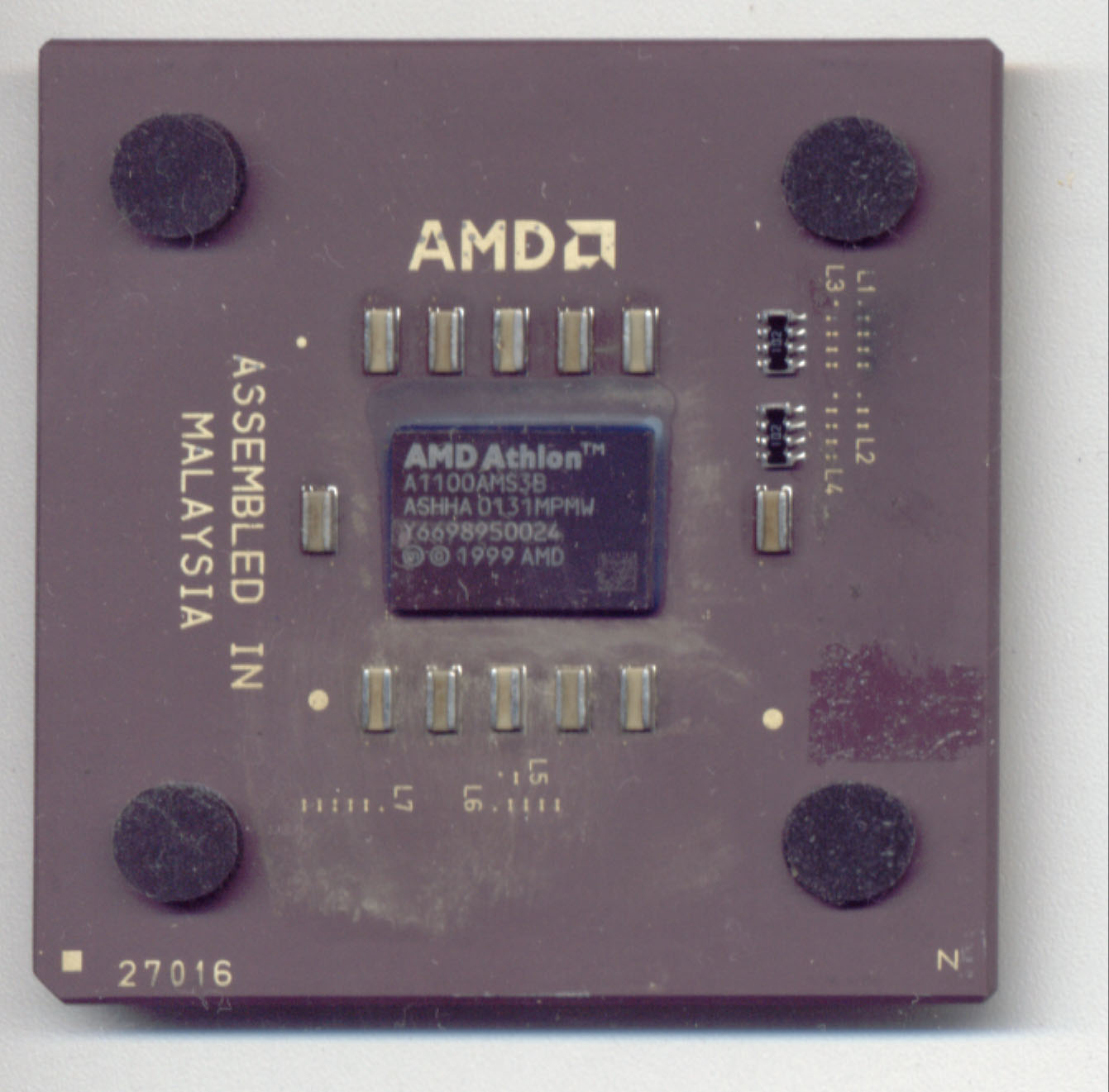
AMD Athlon 1100MHz ASHHA - 2000 The Thunderbird core sported 256kB of on-die L2 cache, but only on a 64bit bus opposed to the 256bit bus of the PentiumIII "Coppermine", the slower cache on the Thunderbird allowing the Coppermine to keep up (just) with Athlon's far more advanced CPU core. This specimen is a dead one, probably burnt or otherwise incapacitated. The Thunderbird was the CPU of choice in 2000-2001, still plenty powerful enough for even light gaming five years later. Though released in August 2000, this particular specimen was manufactured in week 31, 2001 but according to site policy, parts are dated and ordered by their first release in the form they're presented. This Athlon is an early model from the then-new Fab30 in Dresden, using copper interconnects. It overclocked well, hitting 1480MHz on moderately good cooling. Austin parts had a four digit code (E.g. AXDA, my first 800MHz Thunderbird, which ran happily at 1020MHz) and weren't terribly happy over 1GHz. Notably the Thunderbird derivative Mustang, which had 1MB of L2 cache, performed next to identically with Thunderbird, so AMD canned Mustang and brought forward the Palomino project, which was originally what Thunderbird was meant to be, but the Slot-A K7 ran out of steam too soon. The 'Thunderbird' project was to add the rest of SSE (integer SSE had already been added to the first Athlons), improve the translation look-aside buffers and use hardware prefetching to improve cache performance. AMD knew that K7 would be limited by its cache performance but was also limited to a 64 bit wide cache. Short of double-clocking the cache (which would have exceeded the possibilities of AMD's 180nm process), an expensive and lengthy redesign to 128 bit would be necessary, instead AMD made the cache smarter rather than faster. However, the GHz race from 500MHz to 1000MHz was much faster than anyone had predicted and AMD had been forced to take the Slot-A Athlon to 1GHz sooner than they'd have liked. This meant that the Thunderbird project was nowhere near ready when the market was calling for it. Instead, AMD renamed the Thunderbird project to Palomino and rushed out a 180nm Athlon with nothing at all new but 256kB of cache integrated into the die, a rather trivial change. This took the Thunderbird name and was able to beat back Pentium4 long enough for Palomino to reach completion. On release, Palomino was generally 10-20% faster than Thunderbird at the same clock due to its streamlined cache handling. Given that a 1.4GHz Thunderbird was already faster than everything but the scorching hot 2.0GHz Pentium4 (Tbird 1.4 wasn't exactly cool running either) the initial 1.47GHz release of Palomino made Pentium4 a rather unattractive product. Palomino eventually reached 1800MHz.
|
||||||||||||||||||||||||||||||||||||||||||||||||||||||||||||||||||||||||||||||||
| [PENDING] |
Intel Pentium III EB 1,133 MHz QZ64 (SL4HH in retail) - 2000 This is one of the rarer CPUs anyone will ever see. SKU RK80526PZ006256 was recalled very soon after its July 2000 launch. As provided to OEMs it was in the old Slot-1 SECC2 form factor and Intel provided a very high cooling spec for it, and a reference design with a copper base and a very large aluminium vane array, with two 60 mm fans. Other Pentium-III chips on Slot-1 just used a smaller aluminium heatsink and a 40 mm fan. Intel provided it to reviewers with a special VC820 motherboard with a customised BIOS which configured the CPU microcode to run itself quite slowly. In some tests, it was slower than the Pentium-III 1,000 which had been released in March of the same year. A collaboration between Tom Pabst of Tom's Hardware and Kyle Bennett of [H]ard|OCP revealed that the Pentium-III 1.13 was not stable, it would not complete a Linux kernel compile in their testing. Intel's response was quite rapid in recalling the CPU, indicating Intel knew it was a problem before it ever launched. No retail version was ever made, this was purely an OEM/tray processor. My sample has never been powered on and likely will never be. It's a pre-qualification engineering sample with S-spec QZ64. I was working for and with a hardare review site in 2000, during my university studies, and Intel were very keen to get this thing out to as many sites as possible, offering a "review kit" of a VC820 Vancouver motherboard, 256 MB of PC-800 RDRAM, and Intel's own reference cooler (they specifically told us to not use any other cooler). The VC820 was HP-designed, Asus manufactured, and used in some HP Pavilion 1Gs, Dell Dimension XPS B-series, the weird Gateway Vermillion, and a few other OEM machines. The motherboard also proved problematic and was replaced by the D820LP in Intel's recommendations. We didn't ever use the VC820, our FC-PGA 370 board was an Asus CUSL-2 (then, later, the TUSL-2) and our Slot-1 board was the Abit SH6. Intel sent out notice of recall and seemingly wanted nothing more to do with the review kit (this was common back then, the review samples were a 'gift', it was very rare to send them back). We decided not to conduct the review, since we felt it had become irrelevant (that was a mistake at the time), so the kit was unopened for over three years. We'd have used the Abit SH6 and our own 128MB PC-133 SDRAM for repeatability with our other Pentium-III reviews - We weren't about to do a motherboard review, and certainly not one with a one-off beta BIOS!
|
||||||||||||||||||||||||||||||||||||||||||||||||||||||||||||||||||||||||||||||||
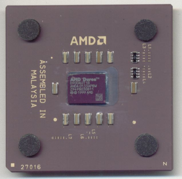 |
AMD Duron 900MHz ANDA - 2001 AMD's Duron (the 900MHz model released in April 2001) was their response to opening a new fab in Dresden. Their older Austin fab was then no longer producing many Athlons, instead AMD cut down the L2 cache on Thunderbird to a mere 64kB and named it 'Duron'. Duron was then sold for ridiculously low prices, one could pick up a 750MHz Duron for around £25, which was just as fast as the Pentium III 733 which cost £70 and only a very tiny amount slower than the 750MHz Athlon (Thunderbird) which was £60. The older Athlon 'Classic' was about the same speed as Duron. The K7 core just never really cared much for cache size, Duron performed within 5% to 10% of the 256kB cache of Thunderbird in almost any test. Up against Intel's very slow Celeron, Duron wiped the floor with it across the board. This 900MHz Duron, paired with PC133 memory, would most likely outperform the 1GHz Celeron below despite a 100MHz clock disadvantage. Strategically, Duron was to win AMD market share and get the market used to AMD as a viable alternative to Intel. Cyrix had been bought by National Semiconductor, purely for the MediaGX, and was run into the ground to the point it was no longer a competitor. AMD found the "Spitfire" Duron cheaper to manufacture than Thunderbird (slightly) and allowed AMD's Dresden facilities to get on with making the high margin Athlon parts, which Austin couldn't do. Duron was a great success, perhaps even greater than the K6-2...But better was yet to come for AMD.
|
||||||||||||||||||||||||||||||||||||||||||||||||||||||||||||||||||||||||||||||||
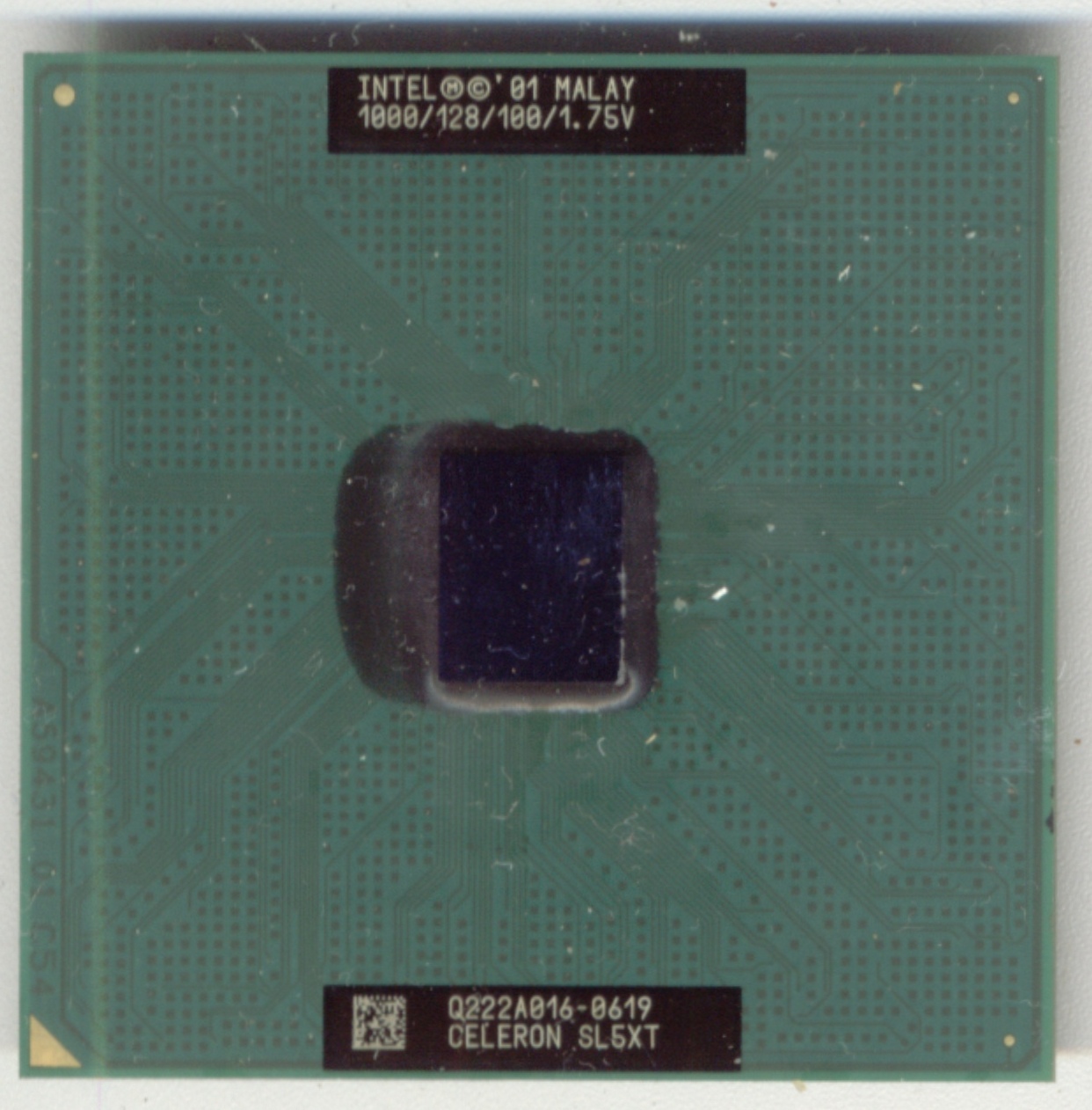 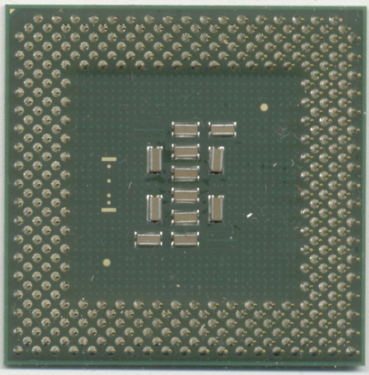 |
Intel Celeron 1000 SL5XT - 2001 The FCPGA 370 Celeron was never something someone would willingly buy. For less money, one could buy a higher clocked Duron when, even at the same clock, a Duron spanked a Celeron silly and was dangerously close to doing the same to the Pentium IIIE. Celeron's problem was one of scaling and, simply, that it didn't. An 800MHz Celeron was about 70% faster than a 400MHz Celeron, but a 1000MHz Celeron from August 2001 was only perhaps 5-10% faster than the 800MHz. Celeron didn't just lose half the L2 cache, but it was also crippled with a dog slow 100MHz bus. The Celeron-T above 1000MHz would rectify this with a 256k cache, but was still stuck at 100MHz. Celerons were, then, nothing more than cheap upgrades for older systems which were stuck on FCPGA 370 (or Slot-1 with a 'slotket' adapter). They were almost always in a cheap VIA or SiS based motherboard, which limited performance even further, with slow RAM and no video card or a very slow one. It was strongly suspected that Intel deliberately limited performance on non-Intel chipsets, either by inadequate bus documentation, or active detection. It was not at all difficult to find puke-boxes from the likes of eMachines using 1000MHz Celerons which were significantly slower than a well built 700MHz Duron. The Duron machine would likely be cheaper too!
|
||||||||||||||||||||||||||||||||||||||||||||||||||||||||||||||||||||||||||||||||
| [Lesser Known] |
Intel "Tualatin" - 2001 Both Celeron and Pentium-III CPUs were made from Tualatin silicon, which was an upgrade of Coppermine. Tualatin reduced bus signaling from 1.5V to 1.25V, which broke compatibility with every existing motherboard (Intel did not want upgraders, since Tualatin was faster than the very profitable Pentium4) in a "don't retain compatibility even if it would be easy to" move. Intel's only supported chipset for Tualatin allowed only 512 MB RAM. Intel seemingly wanted this to fail... On the desktop. Tualatin was the first CPU which was uniquely suited for mobile use as Pentium III-M, it ran much less power at relevant performance, and the Pentium III-S versions were highly impressive for x86 servers. Tualatin had not really done much, but what it had done was very important. The basic P6 core was still the same Katmai core from February 1999 on 250 nm (0.25 micron, as we called it back then). Coppermine had shrunk this core to 180 micron, and added 256 kB on-die L2 cache. Tualatin shrank it further to the 130 micron process, and doubled the on-die cache to 512 kB. Tualatin had also added prefetch logic to the L2$ RAM agent. It was basic and unrefined, but it was far better than nothing and helped populate the L2$ with data before it was even needed. The large L2 cache and the prefetching, as well as low power and fast clocks, made Tualatin a very performant CPU. It was able to hold its own with Athlons of the same clock and, as they did, defeat Pentium4 of hundreds of MHz higher. Tualatin only existed for process reasons. Intel had recently released Willamette, the first Pentium4, on a 180 nm process and it was not doing well. Intel manufacturing had been making P6 for almost five years and were very familiar with it, so requested a P6 design at low volume to trial what they believed was a risky 130 nm process. Lessons learned with Tualatin on 130 nm helped characterise the process for Northwood, the die which brought Pentium4 in from the cold.
|
||||||||||||||||||||||||||||||||||||||||||||||||||||||||||||||||||||||||||||||||
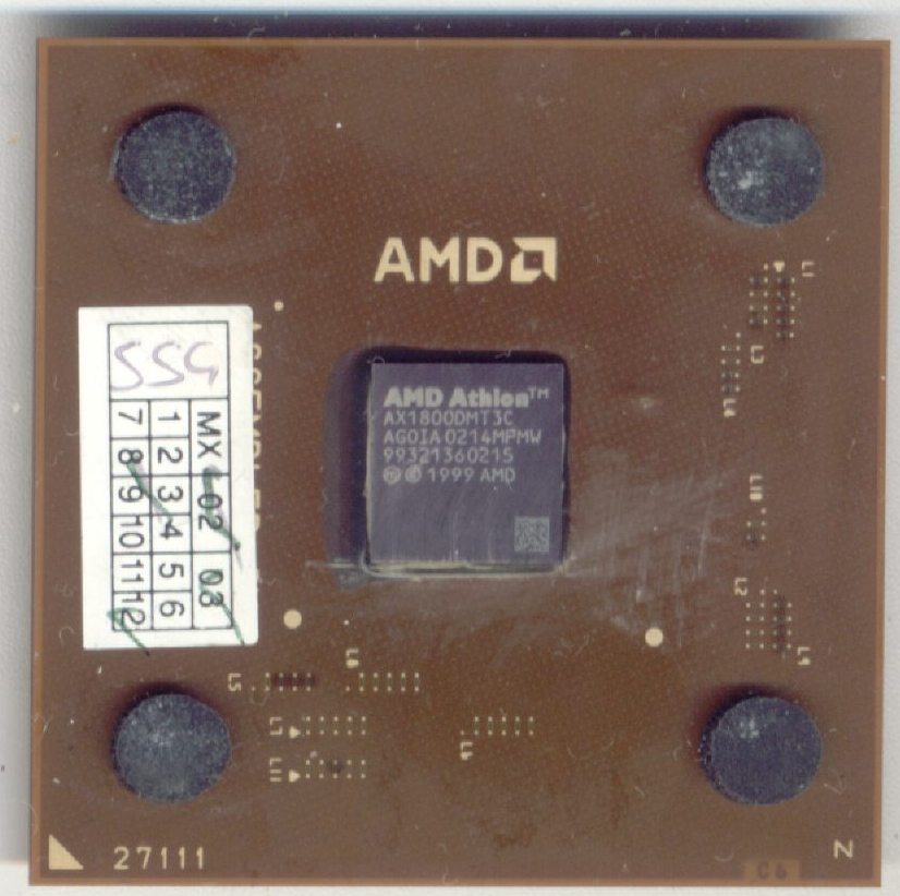 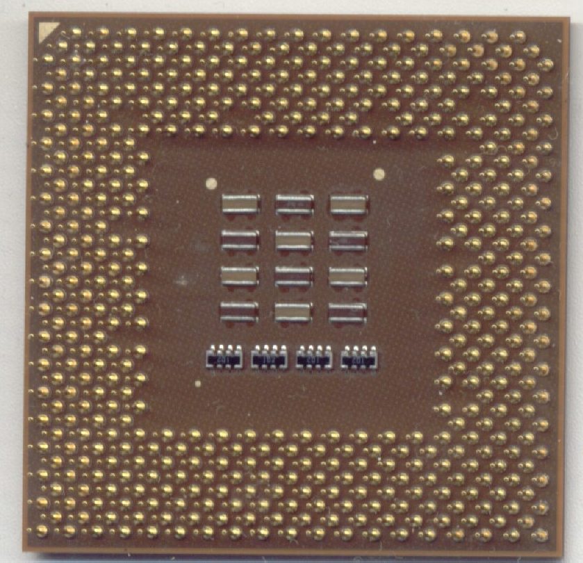
|
AMD AthlonXP 1800+ AGOIA - 2001 The code on this one is AX1800MT3C which tells us it's a 266MHz bus processor at 1.75V and runs at 1.53GHz. That's not important on this model, what is important on this one is the next line down which has the stepping code. The code "AGOIA" may just be random characters to most people, but to overclockers it read "gold". The AGOIA stepping was used in 1600+ to 2200+ processors and practically all of them would clock higher than 1.8GHz. Some made it to 1.9GHz and even 2.0GHz was not unheard of. At the time (October 2001) this the fastest available AthlonXP and the fastest available x86 processor, period. For this particular processor, everything about the model codes yells "great overclocker"; It has the AGOIA code, it is a "9" (third line) and it's a week 13 part. Should it be put back into use, I don't doubt it'd approach and maybe even pass 1.9GHz. Update! This CPU has been put back into use on a motherboard that never supported it, an Abit KT7-RAID, at 1150MHz to replace an old 900MHz Thunderbird. With the stock AMD cooler for the Thunderbird, this CPU hits 53C under full load. The AthlonXP's SSE doesn't work though.
|
||||||||||||||||||||||||||||||||||||||||||||||||||||||||||||||||||||||||||||||||
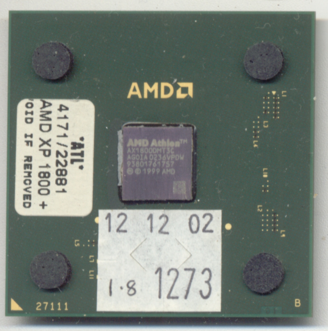
|
AMD AthlonXP 1800+ AGOIA - 2001 Same as above, manufactured in the 36th week of 2002, but in green. The organic substrate AMD used for the AthlonXP was sometimes in brown and sometimes in green, it was pretty random. Both Palomino, both 2002 manufacture (remember, we list by release date, not manufacture date), both overclockable like mad. Back then, green was AMD's brand colour, not red. Red came when AMD bought ATI, which had historically used angry red branding.
|
||||||||||||||||||||||||||||||||||||||||||||||||||||||||||||||||||||||||||||||||
|
Intel Pentium 4 1.8A SL63X - 2002 Pentium 4's 130 nm shrink was Northwood, which also doubled the L2 cache size to 512 kB. SL63X was the original Malaysia production code for the 1.8A, but a later SL68Q code was rumoured to be cooler and more overclockable. Northwood was the first Pentium 4 which was worth buying. Willamette ran very hot, had poor chipsets, poor RDRAM, poor reliability, poor everything. Athlon XP beat it. Athlon beat it. In some cases, Pentium III beat it. Northwood was the first Pentium 4 which pulled ahead of its own legacy, if not ahead of Athlon XP. At this point in history, Intel was openly hostile to PC enthusiasts. Overclocking was banned, multipliers locked, and chipsets even started to not permit bus speed changes. The 1.8A was rated for a 100 MHz bus (quad-pumped to 400 MT/s) but could be configured with a 133 MHz bus (533 MT/s) which would take its 18x multiplier and give 2.4 GHz. Some boards allowed a 166 MHz bus, which would clock Northwood to 3.0 GHz... Going this far needed voltage boosted above 1.7V and was rare. The Abit BD7II was popular for overclocking and a CPU like this could be reasonably expected to reach a 150 MHz bus and 2.7 GHz.
|
||||||||||||||||||||||||||||||||||||||||||||||||||||||||||||||||||||||||||||||||
|
Intel Yamhill |
In around 2002-2004, Intel was known to be working on a 64 bit extension to x86, but didn't want to "Osborne Effect" Itanium, so Intel always referred to it as "memory extension technology", a way to use more than 4 GB natively. Intel had long supported Physical Address Extensions (PAE) and the "NX bit" actually required PAE to be enabled. By 2003, Intel was referring to Yamhill as "Clackamas Technology" or "CT" and Microsoft was referring to "64-Bit Extended Systems". While rival AMD had released Athlon64 and Opteron with AMD64 fully enabled, Intel had had Yamhill present but disabled since at least the "Northwood" Pentium 4 core (130 nm shrink of Willamette with L2 cache doubled) and Intel was planning to enable it in Nocona, the Xeon branding of Prescott (90 nm Pentium 4, minor core changes, L2 cache doubled again). When Clackamas Technology was finally released, it was, well, AMD64. There were some minor differences, nothing anyone needed to care about, and Intel called it "Extended Memory 64-Bit Technology". It didn't hit desktop systems until Prescott-2M (revision of Prescott with 2MB L2 cache). The same Prescott cores also supported "Vanderpool", or Intel's virtualisation extensions. Since Yamhill had been present, if disabled, as early as 2002 and some reports had it present and disabled in Willamette, this would make Intel the first to be shipping AMD64... but didn't enable it on desktop for another four years and still treated it as a premium feature for eight years! |
||||||||||||||||||||||||||||||||||||||||||||||||||||||||||||||||||||||||||||||||
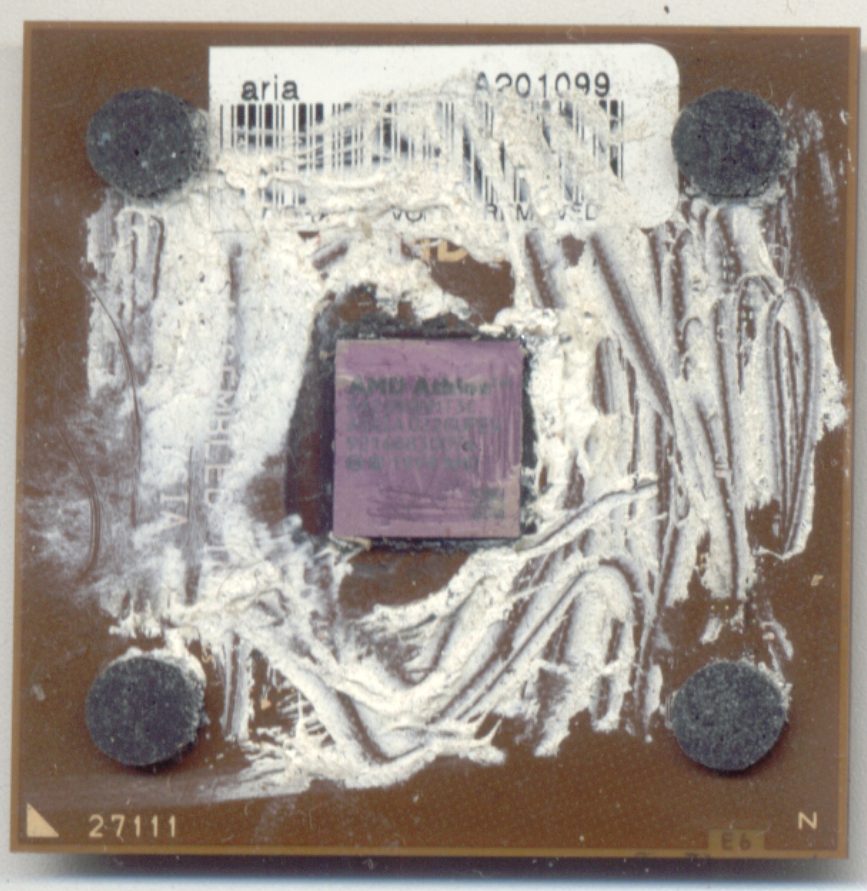
|
AMD AthlonXP 2000+ AGOIA - 2002 Week 20, 2002, AGOIA 9 code...pretty much identical to the above two only for the 2000+ (1.67GHz) rating. Except whoever bought it was a complete idiot and made a hell of a mess of the thermal compound. Don't do this, people. Ever. This one was manufactured not long after its January 2002 release, week 20 working out to be mid-May.
|
||||||||||||||||||||||||||||||||||||||||||||||||||||||||||||||||||||||||||||||||
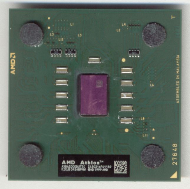
|
AMD AthlonXP 2000+ KIXJB - 2003 The 130nm node for AMD on the K7 core was Barton (below) and Thoroughbred. Barton had 512kB L2 cache, Thoroughbred had 256kB (a "Thorton" version was a Barton core with half the cache turned off, the name is a combination of the two). Most Thoroughbreds were rated to 2400+ and above (1.8GHz) but this one is a rarity, a 2000 rated Thoroughbred. The KIXJB stepping code tells us that it's the Thoroughbred-B core (CPUID 681) redesigned for increased scaling...So why would a Thoroughbred-B be only rated for 1.67GHz? Probably market pressure. It was cheaper to make Thoroughbred-B than it was to make Palomino and the power use of Thoroughbred-B at this kind of clock would be quite low, it was rated for a typical power of merely 54.7W at 1.65V. Thoroughbred-B AthlonXPs at 1700+ - 2100+ were quite rare but by no means impossible to find, especially for mobile applications.
|
||||||||||||||||||||||||||||||||||||||||||||||||||||||||||||||||||||||||||||||||
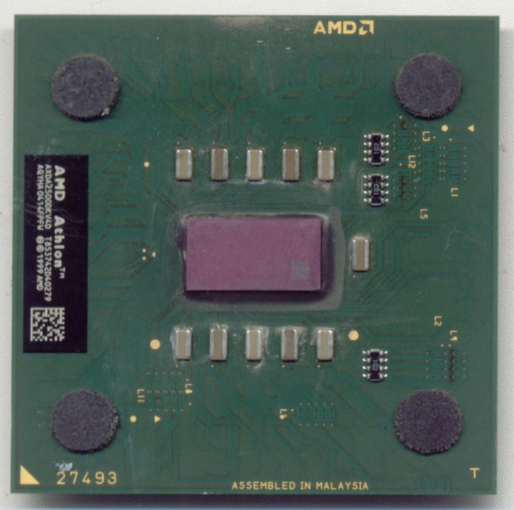 |
AMD AthlonXP 2500+ AQYHA - 2003 Although not a 2500+ Mobile (with the unlocked multiplier) "Barton" part, it shares the same stepping code as the mobiles and was produced in the same year and week (week 14, 2004) as many mobile parts. For overclockers this chip was about as good as it got, able to have its 333 MHz FSB flipped to 400 MHz and the core clock changed from 1833 MHz to 2200 MHz; It became an AthlonXP 3200+ in every way but printing on the substrate. That's exactly why I bought it. This chip served in the main PC, paired with first an Abit KX7-333 (which it was never happy with) and finally an Asus A7N8X-X. When I moved to Socket 939 and an Opteron 146, this pairing remained as a secondary machine. It served well for four years, always with a Radeon 9700 video card, until a heatsink failure finally destroyed it in October 2008. (Not permanently, it seems, it is now on a motherboard and will boot!) There were two 2500+s. The common one was a 333 MHz bus and a 11x multiplier, but a rarer 266 MHz, 14x part existed running at 1867 MHz. AMD's in-house 760 chipset would not run faster than 266 MHz for the FSB, so AMD produced almost all of its AthlonXP speed grades in 266 MHz versions! It was my main machine from 2004 to 2006 always running at 2200MHz and replaced the 1000MHz Celeron in the secondary machine immediately after it was retired from main use. Between its removal from the main desktop and placing as secondary, it was involved in a project to build a PC with absolutely no moving parts. The AQYHA stepping is the highest stepping the AthlonXP was ever produced with. When AMD released them, people soon took note that every last one of them would clock to at least 2200 MHz (I got just over 2.3 GHz with this). These parts continued in production until 2007 as Semprons on Socket A, the final part being the Sempron 3300+ which was identical in every way to the AthlonXP 3200+ - A little bit of ratings fudging from AMD, perhaps. I'm aware of very small quantities of a 2,333 MHz Athlon XP 3200+, which ran on a 333 MHz bus with a 14x multiplier. I've never seen one in the flesh, but these would represent the fastest K7s ever made, or at least ever released. It wouldn't surprise me at all if AMD had some K7s made on 90 nm in the labs.
|
||||||||||||||||||||||||||||||||||||||||||||||||||||||||||||||||||||||||||||||||
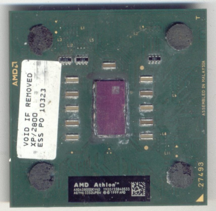 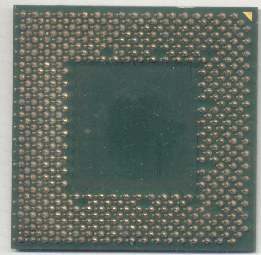
|
AMD AthlonXP 2800+ AQYHA - 2003 The 2800+ represented the sweet spot for people not willing to overclock. The code "AXDA2800DKV4D" tells us the processor is a 130nm AthlonXP (AXDA), it's a 2.0GHz part with a 166MHz bus (2800), the packaging is OPGA (D), it is rated for 1.65V (K), 85C temperature (V), has 512kB L2 cache (4) and the bus speed is 333MHz (D). Model codes aside, the 2800+ was a nippy little processor on the Barton core, which was as advanced as AthlonXPs ever got. Most enthusiasts forgoed the 2800+ for the 2500+, which was also on the 333MHz bus, but when pushed to 400MHz it became a 3200+ and almost all 2500+s made this jump; I say "almost", but I've never seen one which wouldn't. A 2800+ had a 12x multiplier (Socket A provided for a maximum multiplier of 12.5) and would end up at 2.4 GHz if just bumped to a 400 MHz bus. Very few K7 processors were happy that fast. The double size cache on the Bartons didn't really do much for their performance. Ever since Thunderbird, the first socketed Athlons, they were held back by the cache being only 64 bits wide, so being quite slow. Athlon64 would later remedy this with a 128bit cache, but AthlonXP was too early for that.
|
||||||||||||||||||||||||||||||||||||||||||||||||||||||||||||||||||||||||||||||||
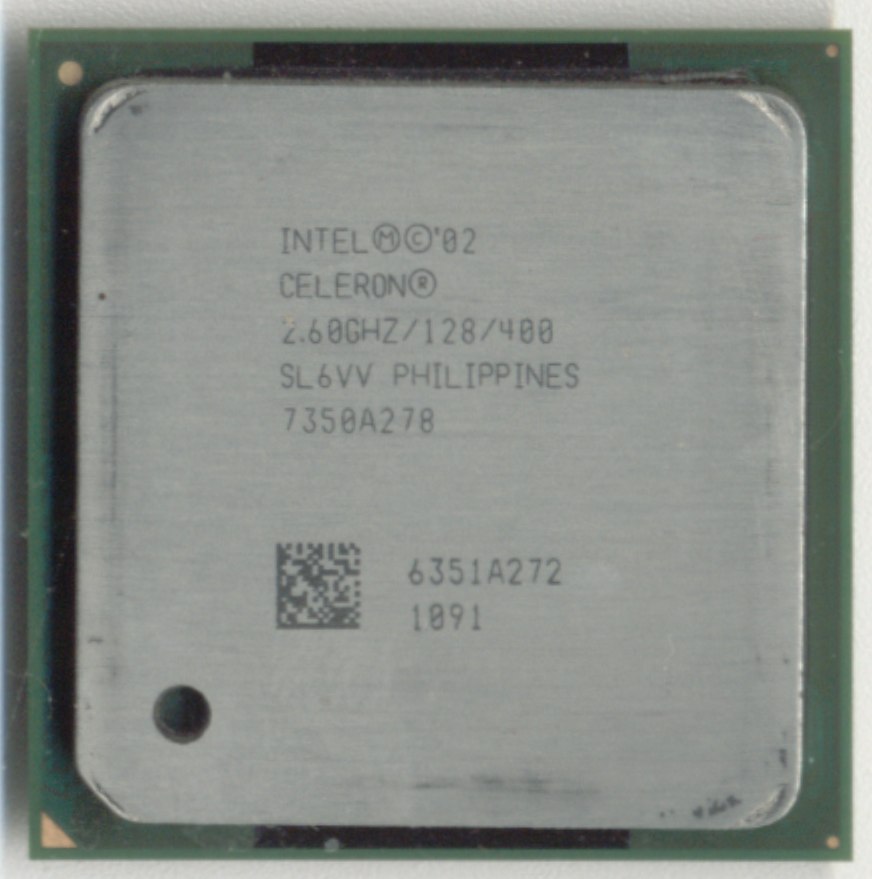 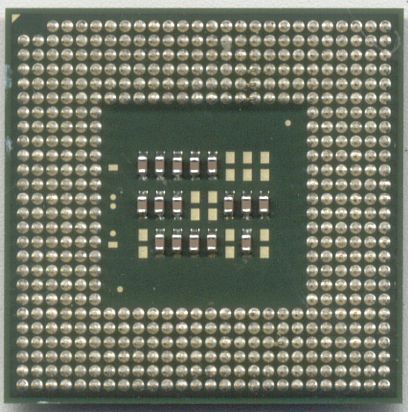
|
Intel Celeron 2.6GHz SL6VV - 2003 This FCPGA 478 Celeron is based on the Pentium4 Northwood core, the 130nm part. It's fairly uninspiring, maybe about as fast as an AthlonXP 2000+ (1667 MHz) in most tests. The FSB is the same 400MHz bus that the P4 debuted with, but the 512kB L2 cache on Northwood has been axed to 128kB (three quarters of it is disabled), see the 2800 MHz Celeron below for more specifics. What's remarkable about this one is not what it is, but where it came from. It came out of a Hewlett Packard Pavilion ze5600. Not tripping any alarms? That's a laptop! This desktop CPU came out of a laptop! It does not support any power management (Intel's Speedstep) which is a dead giveaway. Look up the S-spec if you want more proof. Everything about the laptop was, as its former owner informed me, "crummy". The display was a 15.4" TFT at 1024x768, the kind of panel you find in cheap desktop displays (the laptop equivalent is usually 1280x1024 or higher) and it used the ATI RS200M chipset, perhaps the crappiest P4 chipset ever made other than the i845. I noticed the laptop was thermal throttling under any kind of load, so I took it apart (Service Manual for HP Pavilion ze4x00/5x00, Compaq nx9000 series, Compaq Evo N1050V/1010V, Compaq Presario 2500/2100/1100) and cleaned it up. Taking the heatsink off to clean it I noticed the familiar FCPGA 478 socket, lever and all, for a standard desktop CPU, which is exactly what was populating it, this CPU. I removed it, put the 2.8GHz model in (below), removed the crappy thermal pad (foil and graphite based) and replaced it with thermal paste. On re-assembly, despite the CPU being 4W higher in TDP, it ran between 3 and 8 degrees celsius cooler and didn't thermal throttle at all. One benchmark, GLExcess1.1, went from a score of 938 to a score of 1624 and several games became playable.
| ||||||||||||||||||||||||||||||||||||||||||||||||||||||||||||||||||||||||||||||||
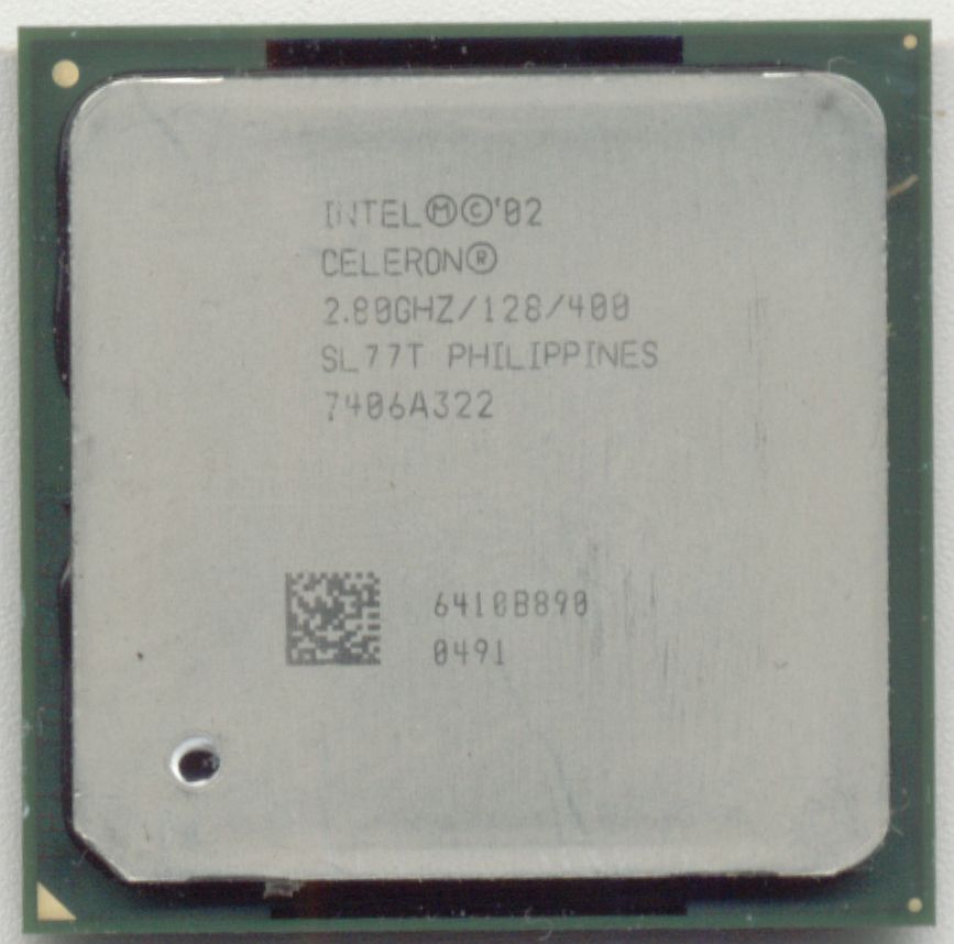
|
Intel Celeron 2.8GHz SL77T - 2003 Intel's Pentium4 based Celerons were even weaker than their PentiumIII ancestors and they were soundly spanked silly by Durons two thirds of their price. The Pentium4 core was quite weak on a clock for clock basis to begin with and it was very sensitive to cache and memory bandwidth. The Celeron had a quarter of the L2 cache of its Northwood big brother and ran on the 400MHz bus (as opposed to the 533MHz or 667MHz of the full Northwood) that the very first Pentium4, the entirely unlovely Willamette, had used on introduction two years earlier. To make matters even worse, they were usually paired with a single channel of DDR memory, usually PC2100 or PC2700. To say it was slow was like saying water was wet. The Athlon XP 2800+ (above) wiped the floor with it for about the same money. It just wasn't sensible to buy such a part. The equivalent performance Pentium4 was around 400 to 600MHz lower in frequency and still available through both OEM and retail channels - For about the same price too! If cost cutting was the order of the day, a cheap motherboard, a stick of PC3200 and an AthlonXP 3200+ was a far better system, cost less and used less power. This one came out of a dead eMachines. No surprise there, then. It got put back into use, replacing the 2.6GHz part just above.
| ||||||||||||||||||||||||||||||||||||||||||||||||||||||||||||||||||||||||||||||||
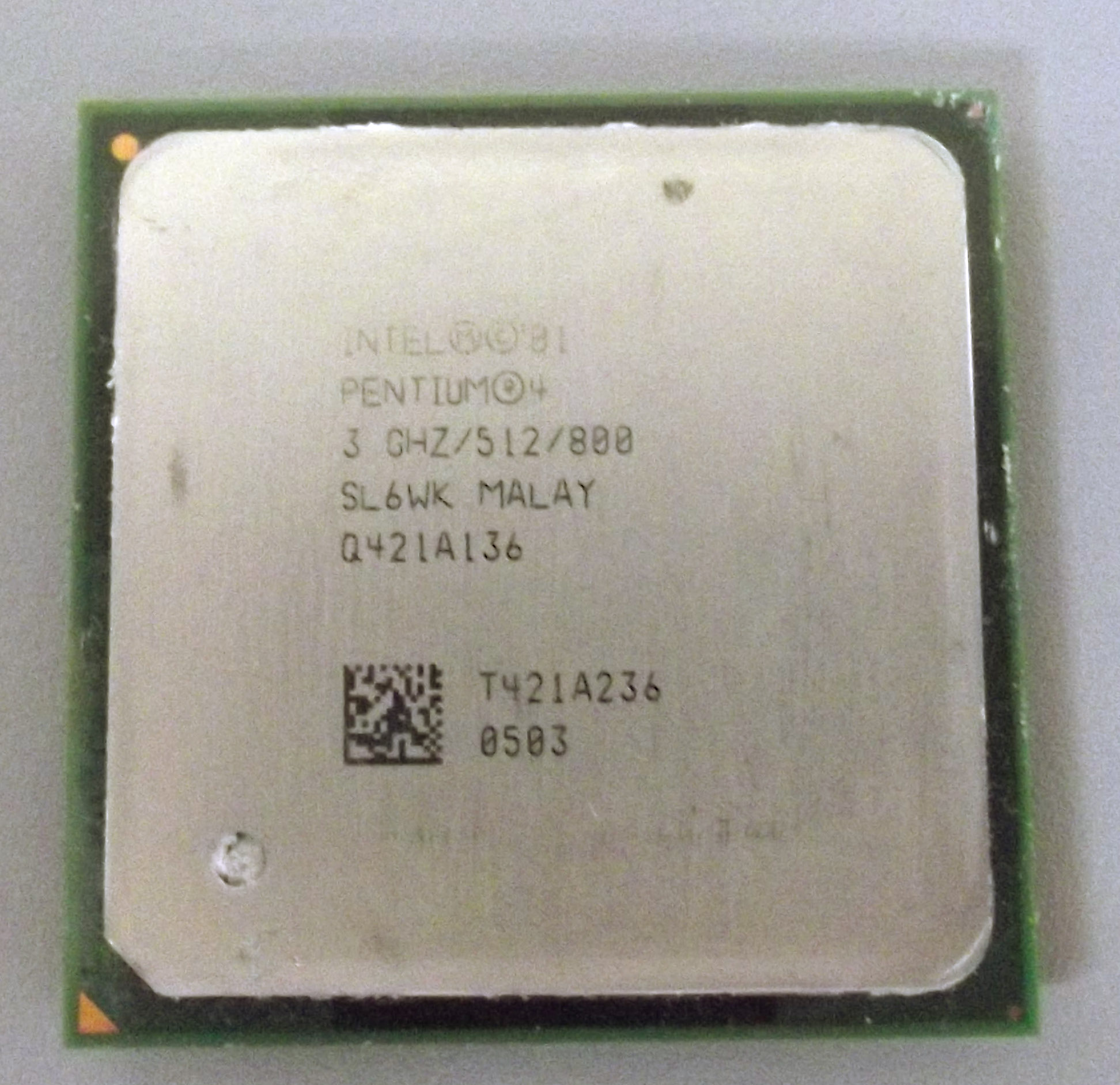
|
Intel Pentium 4 HT 3.0 GHz SL6WK - 2003 This P4 (later re-released as "Intel® Pentium® 4 Processor 745 supporting HT Technology") was about the fastest thing you could put on an Intel motherboard for some time. The 3.2 was faster, but scarily expensive. Northwood was the 130 nm shrink of Willamette, and doubled the L2 cache. Simultaneous multi-threading (SMT, also known as "HyperThreading") was present in Willamette, but never enabled. By 2004, almost all Northwoods had SMT enabled as AMD was, to a word, kicking Intel's ass. SMT on the Pentium 4 was a mixed bag. Some applications saw quite a boost from it (LAME-MT), while others actually saw a performance hit. SMT allowed the CPU to pretend to be two CPUs, so run two threads at once. This placed more demand on caches but theoretically allowed the CPU to remain busy doing useful work if it was waiting on memory for one thread. In practice, the two threads fought each other for cache and the P4's narrow and deep pipelines didn't offer enough instruction-level parallelism (ILP) to allow two to run concurrently. Many speculated at the time that SMT would probably run better on AMD's K8s with their 1 MB L2 cache and much wider execution units, though short of a single in-house prototype I'm aware was made of an SMT-supporting Sledgehammer, we never got to see if this was true. At this time, AMD thought SMT was better done with a multiplication of ALUs, as DEC did with the Alpha 21264, it is not surprising that AMD took a lot of inspiration from DEC, as the chief architect of the Alpha was Dirk Meyer, who was the chief architect of K7 (Athlon), and eventually became CEO of AMD entirely. This thinking would eventually result in Bulldozer. Pentium 4 was, in general, an acceptable CPU. It used a lot of power and ran very slowly in most FP-heavy workloads, but software supporting Intel's SSE2 was much faster on the P4 than anything else. Its major downside was that it was extremely power hungry. This P4 was electrically rated to 112 watts, while AMD's AthlonXP 3200+ (about the same performance) was just 61 watts maximum. With the AthlonXP 3200+ being so much cheaper, as well as on a more mature platform and lacking P4's extreme dislike of some workloads, AMD gained a large amount of marketshare while Pentium 4 was Intel's flagship. Intel on the back-foot, they actually released some Xeons as "Pentium 4 Extreme Edition", the Northwood's "Xeon-relative" was Gallatin, which was identical to the Northwood, but had 2 MB of L3 cache. They were electrically rated as high as 140 watts. Oh, and they cost $999. That's right, one thousand US dollars. And still just a tiny bit faster than a $125 Athlon XP 3200+. Choose the workload carefully, such as some video encoders (XviD was one), and the Athlon XP could be as much as 40% faster than the thousand dollar space-heater.
| ||||||||||||||||||||||||||||||||||||||||||||||||||||||||||||||||||||||||||||||||
| [NO IMAGE YET] |
Pentium-M - 2003 We don't yet have a Pentium-M, but, like the K6-III, the place felt bare without it. As early as 2001, Intel knew the power requirement of the NetBurst architecture was far too high for successful mobile use, yet laptops and notebooks were the fastest growing segment of the market. With the main Sunnyvale-based design teams working on Prescott and Tejas, Intel farmed out the design of a "backup" mobile CPU to a former defence technology contractor in Israel, which had become Intel Haifa and worked mostly on chipsets. The "Banias" project (Banias is an ancient and auspicious religious site in the Golan Heights, important in Jewish and Christian mythology). The team had worked on the memory controller for Timna, which was intended to be Intel's first System-on-Chip, integrating a Tualatin-based P6 core, a basic video adapter (the i754 as seen in i815e), and RDRAM-type memory controller. RDRAM did not work out, so Timna was stillborn after 18 months of development in 1999 and 2000. However, the Intel Haifa team tasked with it had become very familiar with the P6 core and they believed they could get more out of it. This begat the Banias project, where Intel Haifa worked on the largest re-architecture the P6 core had ever seen. P6 had began as Pentium Pro, then was used almost unchanged as Klamath, in Pentium-II (L1 caches were doubled). Pentium-III was a minor revision over Pentium-II, but nothing major architecturally changed in it. Haifa was to take the eight year old P6 and get it caught up. To do this, it was given the quad-pumped GTL+ bus that NetBurst used, to allow chipset commonality. It then doubled the L1 caches to 32 kB each and reduced the longest pipeline path from 14 stages to 10/12 (it depends on the exact path used). Much was made of branch prediction at the time, as NetBurst had a notoriously bad one (it wasn't bad, per-se, it was not effective enough for NetBurst's very long pipeline) and AMD had implemented a state of the art unit in K7. The branch predictor in Banias, no longer as important with a shorter pipeline, had local prediction removed, but was enhanced with the capability of a global history buffer, loop prediction, and the ability to predict some indirect branches. It was almost at the same level as K7. Knowing some instructions decode frequently into common pairs of micro-ops (architectural instructions), Intel added the ability to merge some commonly used instruction pairs into one operation, known as "Micro-op Fusion". Finally, it was the first x86 CPU given proper on-die power management. Previous CPUs could vary their clock multiplier, some even their supply voltage, but these were external factors, and the CPU itself was blissfully ignorant of the outside world. Banias divided its L2 cache into four domains, each of which was only powered when it was active. To make this effective, L2 had to be made large, 1024 kB in Banias. This benefited performance as well as power. On launch, on the 12th of March 2003, the 1.6 GHz Pentium-M was a tiny 83 mm² die with merely 77 million transistors... Running as fast as a 2.4 GHz Pentium-4 "Northwood". While Intel kept stating that Banias was only for mobile, some motherboard makers (Asus in particular) made adapters to run it on desktop. By June 2003, a 1.7 GHz part had been released, which outperformed mainstream desktop Pentium-4 CPUs. Data for Pentium-M 1.6 GHz, the highest launch model.
| ||||||||||||||||||||||||||||||||||||||||||||||||||||||||||||||||||||||||||||||||
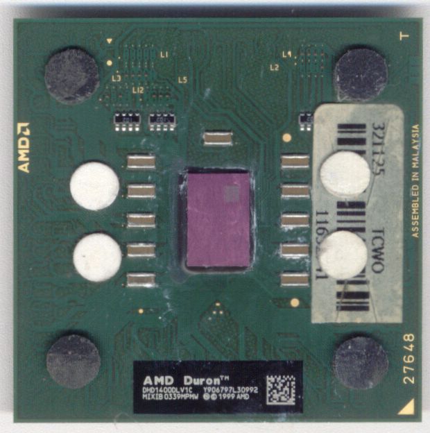 |
AMD Duron 1400 MHz MIXIB - 2004 The Appaloosa Duron part had been cancelled (it was to be a Thoroughbred with just 64 kB L2 cache, as with Spitfire) since it was cheaper to just make more Thoroughbred and turn off some of the L2 cache. Hence this Duron, the last, became known as "Applebred" or, earlier, "Appalbred". Amusingly enough, while the model number of the Athlon XPs were all a sort of performance rating, the Durons were marked with their actual clock. AMD officially stated that it was relative to Athlon-C (Thunderbird) but we all knew it was being measured against Pentium4, especially as benchmark results showed similarly clocked Thunderbirds running quite a bit faster than the "rating" would indicate - the 1.46 GHz XP was rated to "XP 1700+" but a Thunderbird at just 1.55 GHz (the fastest I ever took one) was about the same. A Willamette P4 at 1.7, however, was more or less the same. Odd, that.
|
||||||||||||||||||||||||||||||||||||||||||||||||||||||||||||||||||||||||||||||||
|
|
Intel Pentium 4 2.8E GHz SL79K - 2004 This CPU was found with some e-waste at a fly tipping site (where illegal dumping is done), a T3500 was there, some A/B/G WiFi modules and random laptop parts. It's a 1 MB cache Pentium 4 of SL79K, the cache being 1 MB means it's a Prescott core, it ran at 2.8 GHz, and had an 800 MT/s FSB. This was the lowest model of Prescott on launch, at least non-Celeron, and was the launch C0 stepping of Prescott. Wikipedia has it listed as D0, but as far as I know, only SL7E2 was D0 at 2.8 GHz: Wikipedia lists "Pentium 4 HT" as the correct stepping for this S-spec, but not "Pentium 4", which is just bizarre: All Prescotts supported SMT, as Intel "HyperThreading". Earlier B0 and B1 steppings existed, but none of those went beyond sampling. It was branded as just "Pentium 4 2.8 GHz" Prescott was the logical end-point of the kind of design Pentium 4 represented. On release in early 2004 it had extended the longest pipeline to 31 stages and doubled both L1 and L2 caches. Its 112 mm^2 die was built on a 90 nm process, sported 125 million features, and was branded "Intel Pentium 4 Procesor supporting HT Technology 2.80E GHz, 1M Cache, 800 MHz FSB". The 89 watt thermal design power (TDP) was a little understated, but the higher end 3.4 GHz model it launched with described a 103 watt TDP which was not holding anything back. That particular model was very rare until much later in 2004 and 2005. Prescott was accompanied by a 135 mm^2, 169 million transistor variant which was, weirdly, also referred to by Intel as "Prescott". This larger die had "EM64T" enabled, (Intel's name for AMD64) and 2 MB L2 cache. It was also sold under the "Xeon" branding and was the core taken to 65 nm as Cedar Mill. Intel had stopped giving each die its own name, and now die families shared a name. It added SSE3 instructions to the SSE2 in Willamette and Northwood, and was generally a "Second Generation" NetBurst core, which could have really been called "Pentium 5" but Intel seemingly wanted to keep the Pentium 4 branding, as tarnished as it was. Intel had redesigned the architecture at the same time as moving to a new process node, something which rarely goes well, so Prescott's availability in 2004 remained a little sparse. Intel kept the Prescott P4s priced right next to the Northwoods they were replacing, so this 2.8 GHz was MSRP $178, the same as the Pentium 4 2.8 GHz it replaced. Intel was promising 4 GHz by the end of 2004. Early reviewers were sometimes horrified to find Prescott was extremely power hungry, even compared to the higher Northwoods. An Asus P4C800 motherboard supported both, and they'd run (2.8 GHz model) 72 watts idle and 136 watts 100% load for the older Northwood. Prescott changed that to 107 watts idle and 182 watts loaded. It was incredibly power hungry. The similarly positioned Athlon 64 3400+ (on an MSI K8N SLI) would idle at 71 watts and load up to 115 watts. To try keeping power in check, Intel introduced "loadline B, or "FMB1.0", which allowed the voltage supplied to droop under load, which allowed TDP to drop to 89 watts. Without FMB1.0 support, the CPU would still work, but ran much hotter. In a motherboard which supported it, this was called "Power Optimization". In general business/office tasks, Prescott was a little faster than Northwood, but in Internet performance (things like Java, Acrobat Reader, JavaScript/AJAX/XML, Flash, the staples of 2004's Internet) even Northwood was unable to match AMD's previous generation Athlon XP, and Prescott was far from AMD's Athlon 64. Everything that disadvantaged Intel was turned up in Prescott, so it performed worse than its predecessor. In games, Prescott was mostly slower than Northwood, and both were slower than Athlon 64. Core 2 would remediate this, but was still a twinkle in Banias' eye at this point. This part would be relaunched as the Pentium 4 520 and 521, one described as "2.80E GHz, 1M Cache, 800 MHz FSB" and one described as "2.80 GHz, 1M Cache, 800 MHz FSB". The latter had a minimum voltage of 1.287, the former ran as low as 1.250V. Same platform, both desktop, both 90 nm Prescott, both PPGA478 socket. It was not a great CPU. At this point, Intel had strong-armed most of the chipset market, so the only serious motherboards available with Intel chipsets, meaning they were around 60% more expensive than AMD equivalents. The Athlon 64 it was competing with, therefore, ran faster on a lower cost plaftorm. Ultimately, Prescott failed going forwards. It had increased caches, but the "speed demon" design, which just eked out 4 GHz by 2005, was enormously power hungry and delivered performance no better (and usually worse) than AMD's 2.5 to 3.0 GHz K8. The Pentium 4 architecture had a swan song in Cedar Mill, a die-shrink of Prescott-2M to the 65 nm process at Intel in 2006. Intel's promised 4 GHz? Never really happened. The Pentium 4 580 (1 MB cache) was never released, the Pentium 4 680 (2 MB cache) was never released. Overclocking the 3.0 GHz parts with a 267 MHz bus clock (to give 1066 MT/s) could occasionally give a working 4 GHz, but the 3.0 parts were usually not great bins, since Intel wanted to sell more as the 3.6 and 3.8 GHz components: Prescott-2M's 3.8 GHz part was more than twice the price of the 3.6! The proposed 4 GHz designs were to be a mix of 1066 MT/s bus and 800 MT/s bus parts, but Intel's VRM spec didn't allow for the sheer power draw of Prescott at 4 GHz.
|
||||||||||||||||||||||||||||||||||||||||||||||||||||||||||||||||||||||||||||||||
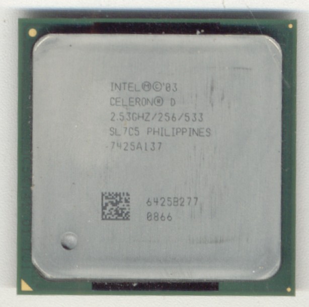 |
Intel Celeron-D 325 2.53GHz SL7C5 - 2004 After the release of Intel's power hungry Prescott core, which didn't exactly set the world on fire (being 10% slower than its predecessor, Northwood), Intel were quick to disable some cache on them and release their Celerons. In this case, the cache was disabled to 256kB from 1MB, exactly one quarter - It was all there, just 3/4 turned off. The 325, as it was later renamed (it was initially just the "Celeron 2.53D"). The very same microarchitectural modifications which made Prescott slower than Northwood also made Prescott's Celerons faster than their Northwood brothers. The L1 cache is doubled in size, the L2 is doubled in size and all Celeron-D parts ran on a 533MHz FSB, up from the 400MHz of their predecessors. This would make it more or less the same speed as the older 2.8GHz part just above. The 2.8GHz part was rated by Intel's rather baroque "TDP" system for 65.4W and electrically specified for a maximum of 87W. The 2.53GHz Celeron-D changed this to TDP of 73W maximum 94W, a common complaint against Prescott was that it used more power even at lower clocks. Indeed, the full Prescott based Pentium 4 3.6GHz was electrically rated to 151W! That kind of temperature from a 112 mm² die made it hotter per unit area than a nuclear reactor.
|
||||||||||||||||||||||||||||||||||||||||||||||||||||||||||||||||||||||||||||||||
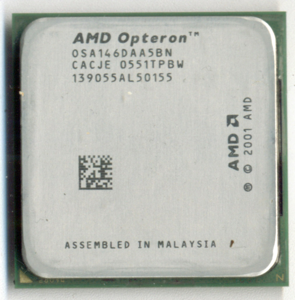 
|
AMD Opteron 146 CACJE 2.0GHz - 2005 At a stock clock of 2.0GHz, the Opteron 146 wasn't really that much faster than the AthlonXP 3200+. It did have faster L2 cache and twice the memory bandwidth, but it was 200MHz behind in core clock. That is, however, where the similarity ends. While the fastest anyone could push an AthlonXP to was around 2.4GHz, the 90nm Venus/San Diego core of this Opteron didn't need anything special to hit 2.7GHz at either 270MHz x 10 or 300MHz x 9; The latter being preferable as it allowed the memory to be cleanly clocked to 200MHz. At those kinds of clocks, it was not at all different to the Athlon64 FX; Same dual channel DDR, same 1MB cache, same 90nm E4 revision core. I wasn't even pushing this one, this particular stepping and date has a very good record for passing 3.0GHz. It simply hit the limits of what my aircooler, six heatpipe Coolermaster Hyper 6+, could handle. The fastest single core processor was either the Pentium 4 Extreme Edition 3.73 GHz or the AMD Athlon 64 FX 57 at 2.8 GHz. Uusally, you wanted the Athlon 64 FX 57. The Athlon 64 FX series were the same silicon as the Socket 939 Opterons, like this Opteron 146, even the same binnings. If anything, the Opterons were better. I ran this guy at 2.72 GHz most of the time: It was neck and neck with the fastest single core CPU in the world. AMD had added SSE2 to the CPU over the SSE supported by AthlonXP, but SSE2 on the Athlon64 or Opteron was little faster than standard MMX or even x87 code. Intel's first Core processor had the same issue: It could run SSE2, but was usually even slower at it. Compared to the earlier Opteron 146 Sledgehammer core (130nm, 2003 release), the new Venus core was 90nm and labelled 'High Efficiency' by AMD due to it using much less power than the 130nm part did when released in early August 2005 - and for Socket 939! Opteron was, of course, underclocked by AMD for reliability and heat. The 2.0GHz AthlonXP used 57.3W under load according to AMD yet, with twice the cache the Opteron 146 was rated for 89W, the exact same as its 2.2, 2.4 and 2.6 brothers, the 148, 150 and 152. It doesn't take a genius to work out that AMD were being very conservative with the Opteron 146, actual power draw measurements under load give numbers around 46-55W. Of course, pumped up from 1.40V to 1.50V and clocked to 2.8GHz, it could easily pass 90-100W. An amazingly flexible little chip which, if allowed to do its Cool-n-Quiet thing and drop multipler to 5x (and voltage to 1.1) when it had no load would happily idle at 1GHz at perhaps two degrees above the system's ambient temperature. Great for a firebreathing gaming machine with the clocks up, great for a silent living room PC at standard. There wasn't much the Opteron 146 couldn't do...except keep up with the inevitable march of technology. This CPU had a short stint powering this server running at 2.7GHz on an MSI K8N Neo2 Platinum without breaking a sweat. It was then sold... Then bought back... Then sold again! It was still in use in 2012. People using Tech Power Up's comprehensive CPU database: It is often inaccurate for CPUs older than around 2013. This E4 Opteron 146 has the wrong TDP (it's really 67 W instead of 89 W) and falsely claims the multiplier was locked. No Socket 939 Opteron had a locked multiplier. CPU World's database is typically more accurate, but often incomplete. I've submitted these corrections to Tech Power Up (in 2018, even) but, as of 2022, it still claims the Opteron 146 was multiplier locked.
|
||||||||||||||||||||||||||||||||||||||||||||||||||||||||||||||||||||||||||||||||
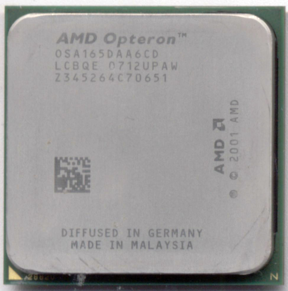 [Back exactly as the 146 above] |
AMD Opteron 165 LCBQE 1.8GHz - 2005 The best of the best Toledo cores, usually from the very middle of the wafer, were selected and underwent additional testing before being labelled as the Denmark, AMD's 1P dual core Opteron. Most of them were sold on Socket 940, usually as upgrades from earlier single core Opterons such as the Sledgehammer or Venus (The Opteron 146 above is a Venus and, believe it or not, released only two days before this dual core part). LCBQE stepping code was later than the CCBWE code, seen from late 2006 through to the last few Opteron 2P HE parts in early 2009. It was Toledo (Consumer), Denmark (Opteron 1P), Egypt (Opteron 8P), and Italy (Opteron 2P). All were 90 nm and JH-E6 stepping. The CCBWE stepping code began in mid-2005 with San Diego and Toledo, but was also seen on Denmark, Italy and Egypt, as well as Roma, the mobile Sempron. Decoding this was simple. In order, the letters meant: Revision/Production: Early Venice was A, most production was C, later was L Configuration: A is 1 core, 1 MB L2 cache, B is 1 core 0.5 MB, C is 2 core 1 MB, D is 2 core 0.5 MB. Even if features are disabled, they'll still be coded here. You wanted codes A or C! IMC Revision: AMD's DDR controller and "uncore", so the system bus interface and HyperTransport, went through numerous revisions. BQ is quite late, the counting works by he 4th letter starting at A and going to Z, then it wraps back to A and increments the 3rd letter. Die Model: Very early Sledgehammer prototypes were seen as B here, but all release chips seem to have been C or above. C was Clawhammer, D was Winchester, E was San Diego, Toledo, etc. and F was Windsor. By the time we got to the "L" codes in Opteron, they were all high end Opteron X2 processors on Socket 940. Some, however, were released on Socket 939 where they represented a high quality, low clock, low heat alternative to the Athlon 64 X2. At heart, all Opterons on Socket 939 were really Athlon 64 FX processors, just underclocked and undervolted so they ran very cool. While this was indeed rated for 110 watts, it would never get there without substantial overclocking. That's not why we bought them. We bought them because they were usually even higher quality parts than the FX series so their maximum clock was usually very high. Around one in five would pass 3GHz and almost all of them would easily pass 2.7GHz. With the Athlon X2s, most overclocking efforts were limited by one core which would run much hotter than the other, a result of being slightly flawed on the substrate (but not faulty). Opterons were selected from parts of the substrate highly unlikely to carry flaws, so both cores were cool-running. Without the handicap of a core being less scalable than the other, Opterons would hit higher clocks. The 90nm AM2 Windsors (JH-F2) were never very happy above 2.8 GHz, yet their Opteron counterparts almost all were capable of 3.0 GHz, regardless of what factory marking they carried. This particular part was manufactured in week 12 2007 on AMD's 90nm process in Dresden, Germany. It ran my main PC on the Asus A8N-SLI Deluxe in the Motherboards section for some time. The stepping code, LCBQE, was first seen in the Opteron 290, a 2.8GHz dual core Socket 940 part. Where most of the Opteron 1xx series were little more than 'overqualified Athlons', the later revisions of them (identified by the code beginning with L rather than C) were genuine Opteron 2xxs which were marked down to 1xx to meet demand (the 2xx series were the same silicon too). They were utter gold. This one was under a by-no-means incredible aircooler (Coolermaster Hyper6+) and was very happy at a mere 2.7GHz. Alas, the motherboard conspired to hold it back since the cooler on the nForce4SLI chip wasn't very good. So at the bus speeds (300MHz+) required for a decent clock, the motherboard itself became unstable. In all, the exact same thing as the 146 above, just E6 (vs E4) revision and dual core. The Athlon X2 equivalent was the 4400+ model. At 2.88 GHz (maximum, the CPU was usually lower due to power management), this CPU is had a two year stint powering the server you're viewing this page from, before being replaced by a Brisbane Athlon X2 4200+ (At 2.52). It would boot quite readily at 3.1GHz but wasn't quite stable there. The fastest Toledo AMD released was the 2.6 GHz Athlon 64 FX-60, this CPU was 280 MHz faster. It was sold and finally became a secondary machine in 2016 when a series of power outages made the machine lose its BIOS settings. The user, thinking it had broken (it lost its boot order), replaced it. People using Tech Power Up's comprehensive CPU database: It is often inaccurate for CPUs older than around 2013. This E6 Opteron 165 does not have a locked multiplier on Socket 939.
|
||||||||||||||||||||||||||||||||||||||||||||||||||||||||||||||||||||||||||||||||
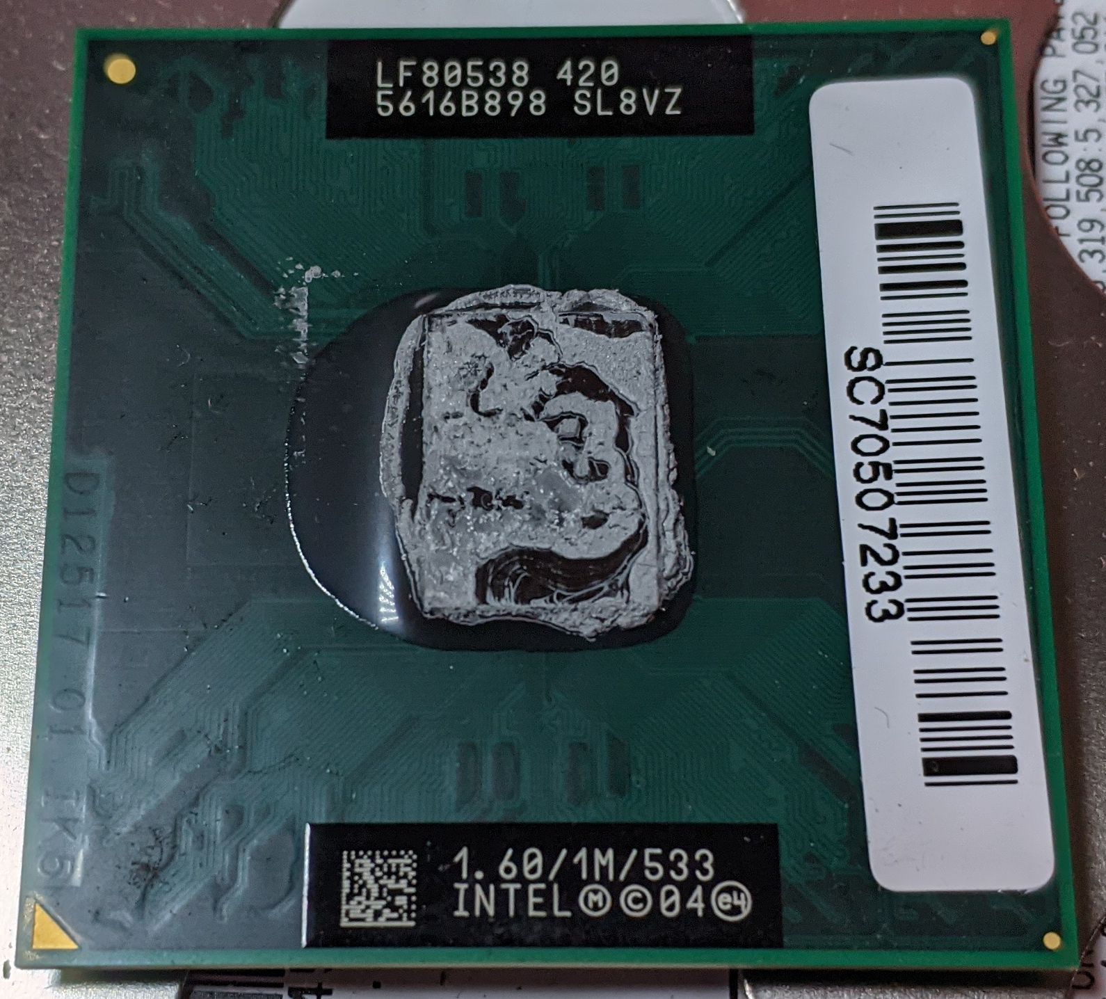 |
Intel Celeron-M 420 SL8VZ - 2006 Celeron-M 420 was around the slowest thing Intel would sell you. It had one Yonah-class core, 1 MB L2 cache, ran a 533 MHz bus and was built on 65 nm. Not that interesting, so the tech writer has to improvise to hold his reader's attention. That's you, good sir. Celeron-M 420 had an "SL8" S-spec, and Celeron-M 430 was an "SL9", so there was clearly some difference. What was it? The core stepping had moved from C0 to D0 with SL9 specs, but was the same Yonah-1024 single core, 1 MB die. The stepping doesn't appear to have changed much. Intel also changed the capacitor layout on the rear of the CPU from C0 to D0. In mobile, Yonah-1024 replaced Celeron-D and Mobile Celeron parts, which were based on the Pentium4 architecture, power hungry, inefficient, low performance. The 1.6 GHz Celeron-M here would run software at around the same speed as the 2.53 GHz Celeron-D 325 just above.
|
||||||||||||||||||||||||||||||||||||||||||||||||||||||||||||||||||||||||||||||||
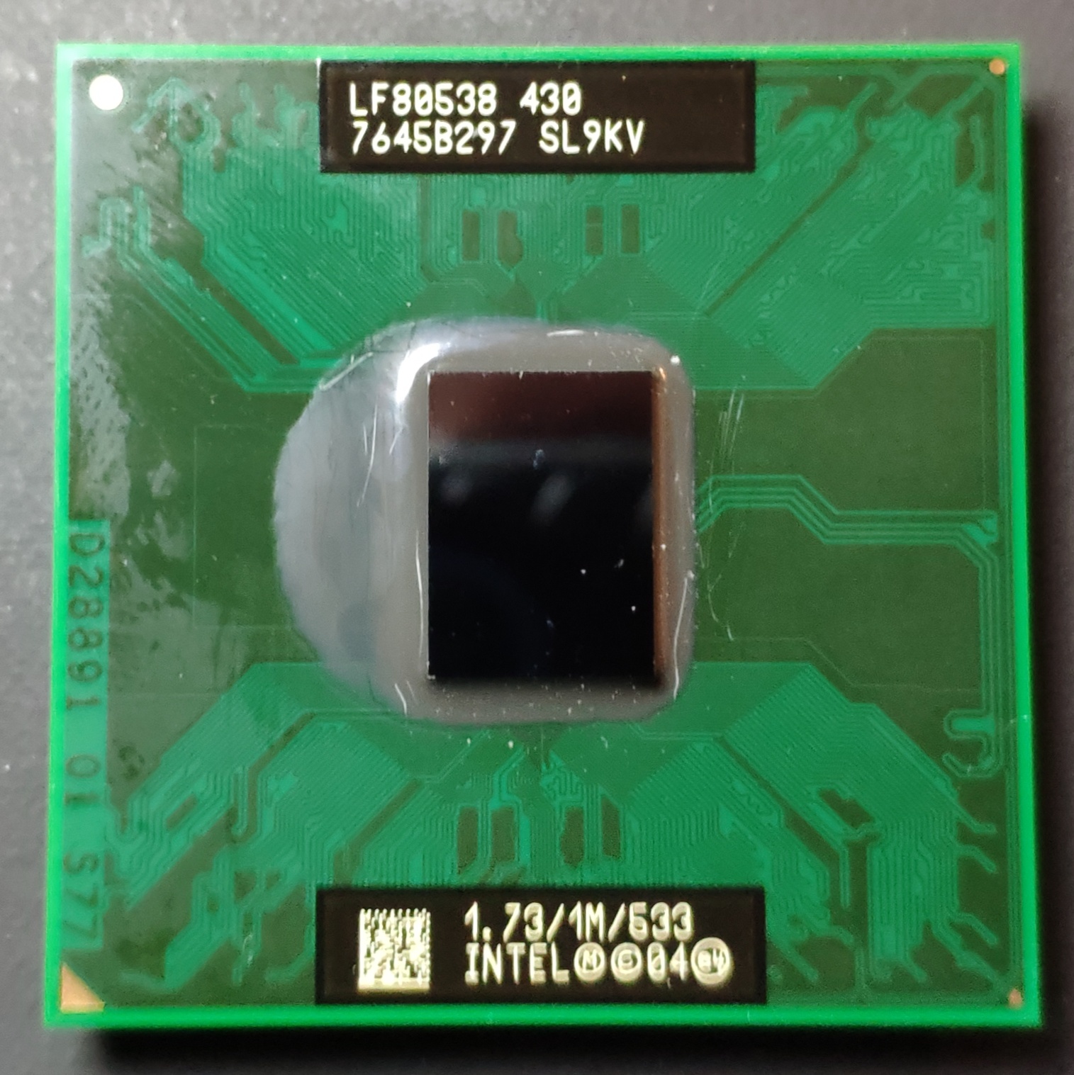 |
Intel Celeron-M 430 SL9KV - 2006 In January 2006, Intel dropped the unassuming Core Duo and Core Solo parts on the market. They were mobile only, like all the Banias derivatives. April saw the first three Celeron-Ms drop, the 410, 420 and this 430. Being designed by the Intel Haifa team, these all had religious codenames: "Banias", the core architecture, is the site Yeshuah Masiah ("Jesus Christ", translated) claimed to Peter that he would build his church. "Merom" is a type or level of heaven, and "Yonah" is the Hebrew for "dove", important in religious symbology. Intel made two silicon variants of it, Yonah and Yonah-1024. The former was dual core and 2MB L2 cache, the latter was half of both. From the size of the die here, around the same as Merom-L, this appears to be the full Yonah with a core and half the cache disabled, instead of not present at all. It's hard to say for certain without good images of both. At 27 watts TDP, Celeron-M 430 was very good for a mainstream mobile part and wiped the floor with Intel's Pentium4 Mobile.
|
||||||||||||||||||||||||||||||||||||||||||||||||||||||||||||||||||||||||||||||||
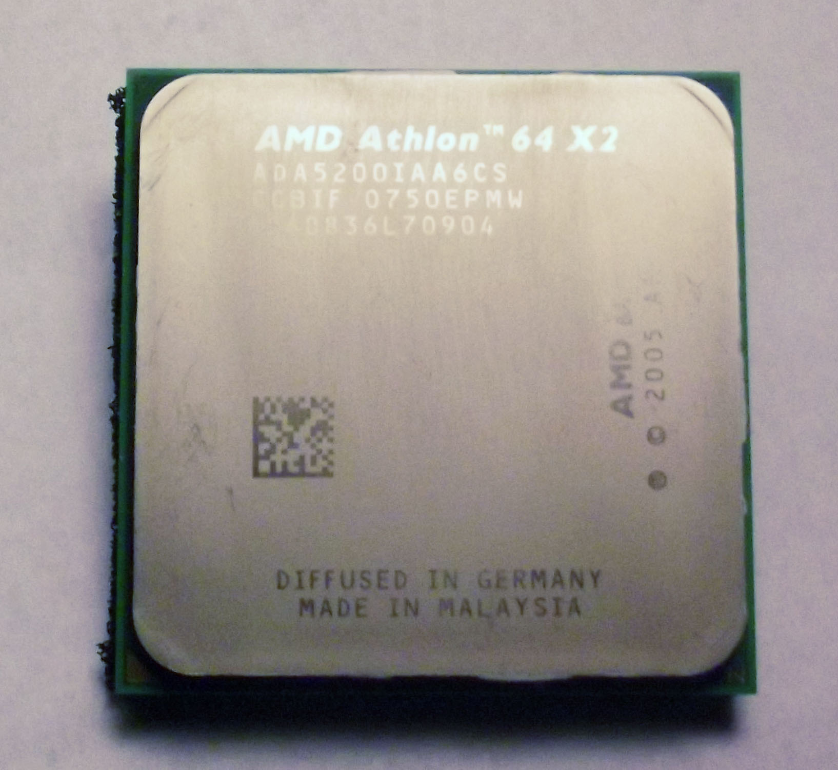 |
AMD Athlon 64 X2 5200+ CCBIF - 2006 AMD's Windsor core, at 227 million transistors (see note) was the introductory part for AMD's AM2 platform, supporting DDR2 memory. The performance difference was, to a word, zero. All the initial AM2 parts were to the "FX" spec, of having the full 1 MB L2 cache per core, though later 512 kB parts arrived, either as Windsor with some cache disabled or Brisbane, the 65 nm shrink. Confusing matters was that there were two different 2,600 MHz parts, the 5000+ Brisbane or the 5200+ Windsor, and two different 5200+ parts, the 2.6 GHz Windsor and the 2.7 GHz Brisbane. AMD thought that half the L2 cache was about the same as 100 MHz core clock, with some justification. Confusing matters more was that some Windsors were marked as Brisbane, ones which had 512 kB cache natively and none disabled but were still the 90 nm part. This part had no "codename" and was also called Windsor. A weird 3600+ 2 GHz model (Athlon 64 X2 3600+) had just 256 kB L2 per core and was variously made using 1024 kB or 512 kB silicon. In June 2006, AMD announced it would no longer make any non-FX processors with the full 1 MB cache, although they still trickled through until 2008, this one is marked as being produced week 50 2007 and was bought mid-2008. The dies seemed to exist as just two units: A very large almost square one and a smaller rectangular die. The larger one was the 1024 kB L2 version, the smaller one was the 512 kB variant. The actual silicon being used was named per its featureset, not what was being manufactured, except when it wasn't. It was bizzare, confusing, and the below isn't with full confidence. AMD used the same Athlon 64 X2 xxxx for all these products, except some of the later 65 nm parts, which dropped the "64" as just Athlon X2.
Manchester was an oddball. It was a revision E4 - same as San Diego and Venus - but dual core. The probable explanation would be that Manchester was not "true" dual-core, but half-cache San Diegos on the same substrate, but a de-capped Manchester was a monolithic die. Additionally, some E6 (Toledo) CPUs were marked as Manchester with half their cache disabled. Most Manchesters were likely actually Windsor silicon. Quite a lot of 512 kB Windsors were actually the 227 million, 1024 kB part with half the cache turned off. For some reason, AMD had a lot of yield problems with Windsor, which it did not have with Toledo on the same 90 nm SOI process. Toledo would almost always clock higher and run cooler, but it was Windsor which was in the highest bins. Performance was per clock identical to the Socket 939 Opteron 165 above, while the DDR2 AM2 socket had more bandwidth available, it was higher latency and AMD's DDR2 controller was really not very good. It wasn't an upgrade for me, though. I was replacing the Opteron 165 above (I broke the Socket 939 motherboard), which ran at 2.8 GHz. This Windsor would just run at 2.8, but needed a huge core voltage boost to do so, and ran very hot. The F2 revision was never produced faster than 2.6 GHz and F3 only made it to 3.2 GHz. Oddly, the 65 nm Brisbane was never released that fast, its highest bin being 3.1 GHz for the fantastically rare 6000+. My own Brisbane (a 4000+, 2.1 GHz) will not clock past 2.7 GHz no matter how hard it is pushed. Usually a die shrink means higher clocks, but AMD's 65 nm process or its DDR2 K8s seemed to just not work very well. Most likely, the critical path optimisation needed to get more clock out of K8 just wasn't worth it. After AMD's success on the 90 nm fabrication process and it using the same designs on the 65 nm process, observers expected great things. Surely if most of AMD's chips on 90 nm would approach 2.8 GHz, some hit 3.0 GHz, then 65 nm would mean AMD would be able to push 3.5 GHz and more. 65 nm did not appreciably reduce power, did not appreciably increase clock headroom, in fact the majority of 65 nm Athlon X2 chips would not clock as high as their 90 nm brothers, ran hotter and were never quite as happy when overclocking. The Brisbane 4000+ that replaced this 5200+ wouldn't go much beyond 2.6 GHz, for example. The only explanation is that AMD's 65 nm silicon-on-insulator process node was just bad.
|
||||||||||||||||||||||||||||||||||||||||||||||||||||||||||||||||||||||||||||||||
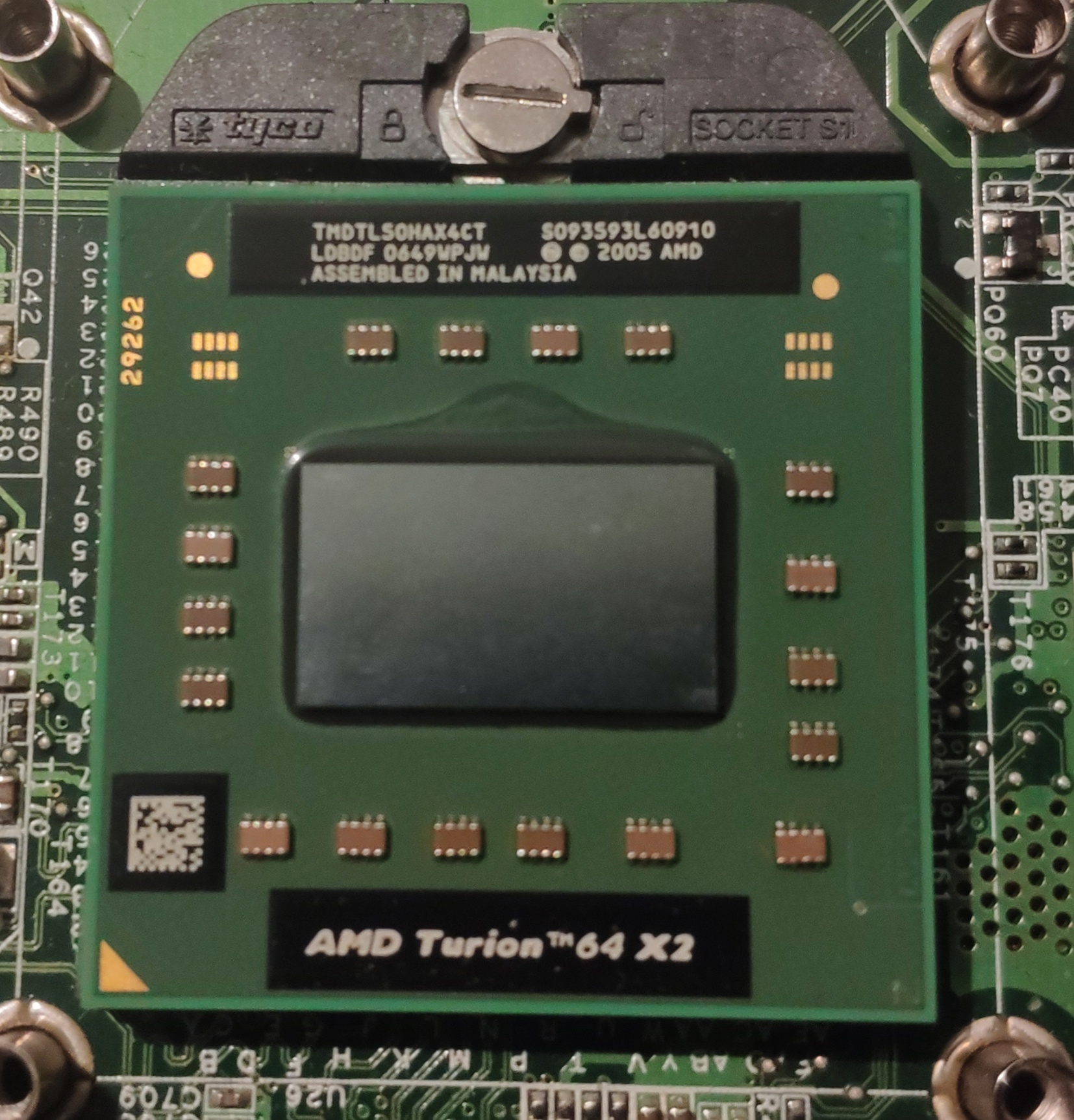 |
AMD Turion 64 X2 LDBDF - 2006 Turion was the brief branding AMD did for some late K8 and the mobile/embedded K10s. The part code TMDTL50HAX4CT tells us it is the TL50 model with the core name "Taylor". There was also the overlapping name "Trinidad". It is seen here nestled in Socket S1, where it ran at 1.6 GHz on an 800 MHz HyperTransport bus. It used 90 nm manufacturing technology and sported 153.8 million transistors. L2 cache was 256 kB per core. On the desktop, this exact silicon was called "Windsor" and usually branded Athlon X2. Desktop variants had all 512 kB per core L2 cache enabled, but only the "Trinidad" mobile versions had all the cache turned on, "Taylor" was cut back quite a lot. The 638 pin Socket S1 was AMD's first ever mobile-only socket, before then AMD had used Socket 754, Socket A, and even Super 7. This was not unusual, Intel had also used Socket 370 and the semi-compatible FCPGA 370 on laptops and, at the time, was using the desktop Socket 478 in laptops. Socket S1 went through four generations: S1g1 was equivalent to Socket AM2, S1g2 was equivalent to AM2+, S1g3 equivalent to AM2+, and S1g4 is comparable to AM3. It was a quite reasonable way to get the extra responsiveness of a dual core on a mobile machine, particularly when high CPU performance was not needed. Thermal design power was 31 watts, which was high for a mobile of this performance.
|
||||||||||||||||||||||||||||||||||||||||||||||||||||||||||||||||||||||||||||||||
 |
Intel Celeron-M 540 SLA2F - 2006 Intel's Merom was the mobile name for Conroe, the desktop dual core Core 2, or Woodcrest, the server Core 2. Merom, Merom-L and Merom-2M existed. Merom-L had one core and 1 MB L2 cache. Merom had two cores and 1 MB L2 cache. Merom-2M had two cores and 2MB L2 cache. All examples used the existing Yonah CPU architecture, developed by Intel in Israel. Yonah used shared L2 cache between the two cores. The shared L2 cache made the design powerful, but also monolithic. It wasn't easy to synthesise into a silicon design without making a completely new design, so Intel kept the number of distinct dies down. Sandy Bridge was to revisit and resolve this issue as one of its "configurability" design goals. This SLA2F part was Merom-L, one enabled core, 1 MB L2 cache, 533 MHz bus. Enhanced C1E power management and SpeedStep were disabled, so Celeron-M used much more power than it really needed to. This was to prevent its use in lighter machines with longer battery lives, as Celeron and Intel's Core 2-ULV were dramatically overlapped. Merom was Intel's first ever "Tock" in the "Tick-Tock" paradigm, where a "Tock" was a new architecture on an existing process, and a "Tick" was the same architecture on a new process. Merom's corresponding "Tick" was Penryn on 45 nm. Merom had many silicon variants, so three configurations were all "Merom" - Dual core 4 MB, dual core 2 MB, and single core 2 MB, which were "Merom", "Merom-2M" and "Merom-L" respectively. All of these were also called Conroe or Woodcrest if they were aimed at the corresponding segment... Intel was more of a marketing company than a manufacturing one, it seemed! This Celeron-M 540, for example, used both Merom-2M (Allendale) and Merom-L silicon.
|
||||||||||||||||||||||||||||||||||||||||||||||||||||||||||||||||||||||||||||||||
 |
Intel Celeron-M 570 SLA2C - 2006 This Merom-L product ran at 2.26 GHz and made a decent entry-level laptop, but if we're on a Celeron-M, we probably have already made many sacrifices already and the CPU won't be the limiting factor. This came out of a Fujitsu-Siemens with 2 GB RAM (2x1GB, so at least in dual channel) with a horribly slow Seagate Momentus hard drive. It's a speed grade of the one just above. If you want details, they're there.
|
||||||||||||||||||||||||||||||||||||||||||||||||||||||||||||||||||||||||||||||||
  Click for a 4k version! |
Intel Core 2 Duo T7200 SL9SF - 2006 Another Merom processor, this time the full on dual core, 4 MB L2 cache model. It's plain that different silicon is in use here, highlighting the difference between Merom and Merom-L.  The 4 MB L2 cache Core 2 Duos were worryingly powerful on release, not only catching up to AMD's Athlon 64 FX and Athlon X2 processors, but soundly pulling ahead of them. While AMD had faster, lower latency memory thanks to the integrated on-die memory controller, Intel just threw a huge big dumb L2 cache at the problem. Pentium 4 was wholly unable to keep up with AMD. Core 2 didn't just keep up, it pulled ahead. This sample was pulled from an elderly Dell Latitude D620 where, as can almost be seen in the background, it got to play with an Nvidia Quadro NVS-110M... A slightly knobbled Geforce Go 730, which in turn was a castrated GeForce 7200 GS. It was better than the IGP and, well, that's about it. It feels wrong to end the piece on a negative about an unrelated product, so we'll instead mention that the performance of the T7200 was sufficient that this laptop was a casual user's daily driver until well into 2015, with 2 GB RAM and Windows 7. At that point, 2 GB just wasn't enough and the Dell D620's keyboard was beginning to fail and the Intel 945PM chipset was picky about its RAM support, so an upgrade to 4 GB was passed over in favour of a replacement device.
|
||||||||||||||||||||||||||||||||||||||||||||||||||||||||||||||||||||||||||||||||
 |
IBM Broadway-1 (65 nm) - 2007 This tiny little guy, under a cap merely 15 mm square, bears markings that it was made in 2010, week 52, so was beyond the 2007 point when the original 90 nm Broadway's already tiny die was shrunk to 65 nm. Nintendo made much about how the Broadway CPU was "specially modified for the Wii", which meant it was a variant IBM didn't have as a standard SKU. It was a PowerPC 750CL. So, let's examine what this is? What seems like a million years ago, Motorola introduced an entry-level PowerPC processor to supplant the PowerPC 603e, running the 600-series system bus faster at 66 MHz, doubling L1 caches to 32 kB each, adding a second integer pipeline, branch prediction, and, for the 750, a back-side bus for L2 cache, 256, 512 or 1024 kB. Apple used it as the "G3" in the Power Mac G3 and iMac. On IBM's 260 nm process, it measured a tiny 67 mm². The 740 and 750 were the same silicon, but 740 altered the pinout to disconnect the back side bus. It shared the same pinout as the 603e and so could be a drop-in replacement. IBM continued development of PowerPC 750 far beyond its beginnings. The 745 and 755 were direct die shrinks to 220 nm (51 mm²) in 1998, while in 2000 the 750CX was released, integrating 256 kB L2 cache on a 43 mm² die. Apple used this sparingly, in a single iMac model. The 750CXe bumped clock even further, using gains from the 180 nm process, and improving the floating point unit. As the "Gekko", the 750CXe had a subset of AltiVec added to its 43 mm² die... Take a quick note here: The feature set and basic design was frozen here for Broadway. The 750FX (2002), 750GX (2004), VX (cancelled when Apple abandoned PowerPC) extended 750's feature set but IBM canned that lineage when their market, purely Apple, vanished. IBM's industrial, aerospace, and military customers wanted CXe and FX. 750FX powers Boeing's "787 Dreamliner" widebody airliner as part of the same Honeywell aerospace computer Boeing also chose for the cursed Orion Multi-Purpose Crew Vehicle. We've taken a wide sidetrack here, but now come back to PowerPC 750CL, which is a derivation of 750CXe, which was a die-shrink of 750CX. All three were made in the same 20 million transistors, and the 750CL was down to a die size of 16 mm²! As "Broadway" and it ran at a weird 729 MHz, but clock speed can be easily and trivially changed. The 18.9 mm² (4.5 x 4.2 mm) die was larger than the regular 750CL due to Nintendo specifying a low power (lower density) manufacturing process. It used around 2 watts, the actual figures not made public. The 729 MHz clock wasn't some special magic by Nintendo. Nintendo was building a console, not a CPU, and the CPU was not important. The GPU was. All consoles since around the fifth generation have been about video performance, and that's where the priority is. On the Wii motherboard, the Hollywood GPU package was the RAM controller, timings generator, system bus controller, I/O controller, and clock generator. As it ran at 243 MHz, a simple 3x multiplier got the 750CL running at 729 MHz.
|
||||||||||||||||||||||||||||||||||||||||||||||||||||||||||||||||||||||||||||||||
 |
Core 2 Quad Q6600 - 2007 Q6600 was the high end CPU to have in 2007. It was a multi-chip-module (MCM) based around two Conroe dies: Conroes intended for embedding into a quad were known as "Kentsfield". It was built on Intel's 65 nm process and was rated to a 105 watt TDP. The two Conroe dies had 4 MB L2 cache each and the CPU ran at 2.4 GHz from a 1066 MHz (4x266) FSB. That's all a bit dry. Conroe was an overclocking beast. Most of them would trivially pass 3.0 GHz. Some samples were able to approach 4.0 GHz. Some passed 4.0 GHz. Intel back then did not permit overclocking on anything, so all multipliers were locked, and overclocking was done by raising the FSB speed This one was tied with an Asus P5E motherboard (a slightly less featureful Maximus Formula) and 8 GB DDR2-800 RAM. Even in 2010, that was a worthwhile machine... Particularly with some overclocking! Kentsfield and Conroe were regarded as legendary CPUs and firmly took back the performance crown from AMD, which had had it for nearly a decade. | ||||||||||||||||||||||||||||||||||||||||||||||||||||||||||||||||||||||||||||||||
 |
Intel Core 2 Quad Q8300 SLGUR - 2008 Like other Core 2 Quads, these slightly reduced parts were made from either two Wolfdale dies or a single Yorkfield die. With the reduced L2 cache and slightly lower clocks, gamers typically preferred faster Core 2 Duos, such as the C2D E8400. In either case, the two dual-core modules are wholly independent and connected only via the front side bus. AMD made much of this, saying they were not "true" quad cores. AMD would have more of a point if its own 2008 offerings of Barcelona were any faster. AMD was vindicated, however, as all multi-core processors today have a large shared L3 cache, which AMD introduced with the ill-fated Barcelona.
|
||||||||||||||||||||||||||||||||||||||||||||||||||||||||||||||||||||||||||||||||
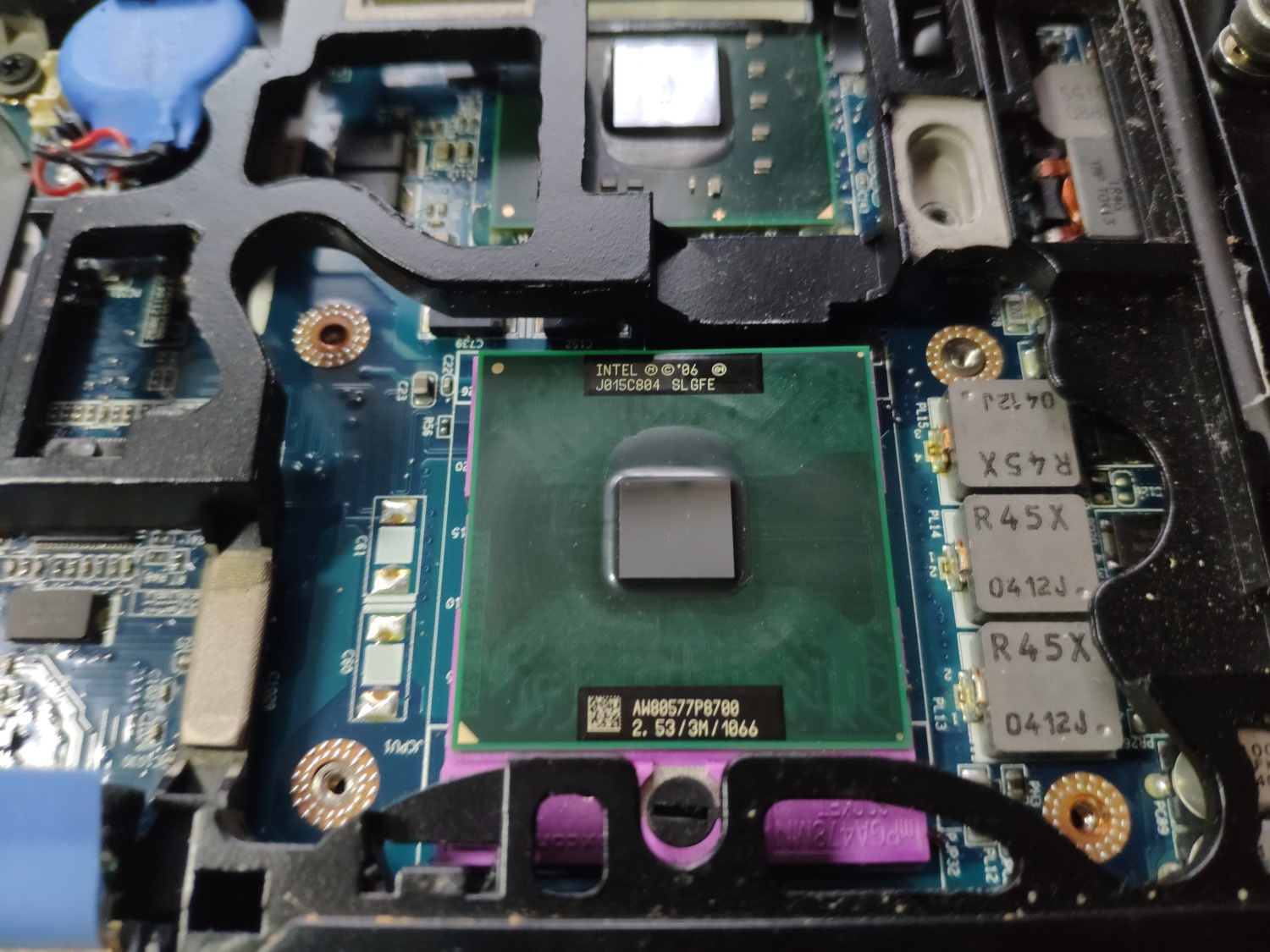 |
Intel Core 2 Duo P8700 SLGFE Socket P was Intel's mobile socket, where the surface mounted FC-BGA478 package wasn't used. With a 25 watt TDP, Penryn-3M was a tiny 82 mm^2 die (Full Penryn was 6 MB L2 cache and 107 mm^2) and actually smaller than the chipset which supported it. Penryn was a die shrink of Merom, with Merom's 2/4 MB L2 cache options changed to 3/6 MB. The desktop Wolfdale was the same 107 mm^2 silicon as Penryn. Penryn-3M was Wolfdale-3M on the desktop. They were identical. The whole product line was referred to as Kentsfield. We see it here mounted in a Dell Latitude E6400, still working at 11 years old in 2020, slow but functional in Windows 10. At the time, these were the mobile CPUs you wanted. Laptops were still a generation or two from having reasonable video performance, even as some of them sprouted power-hungry discrete GPUs. Intel's mobile platform was awful, but everyone's was. The Cantiga-GM (82GM45) chipset was rated for 12 watt TDP with the ICH9M adding 5 watts to that. Intel was in the business to make money, not good laptop chipsets, so the chipset was a desktop part (Cantiga was Eagle Lake on the desktop) ran at a slightly lower voltage and clock rate to drop the power from 22 watts to 12 watts, cut the 1333 MHz FSB, and de-clocked the GPU, but also manufactured on older lithography - likely 90 nm in this case. This enabled the production of products in older, paid-for, foundries. Of course they use twice the power they needed to, but where else are you going to go? The P8700 itself was rated at 25 watts. Flat out, this is almost 45 watts just on the CPU and chipset. If we go back to 2008, when this was all new, 45 watts mobile was tolerated. It was okay for a performance or mainstream mobile platform. Nobody liked it, and it was the reason why laptops were only expected to run on battery for 2-4 hours, but this Dell and its 45 watt-hour battery would run for those 2-4 hours. The Latitude E6400 was serious kit, built for easy and rapid service, the keyboard drains into drain channels for liquid spills, and is a field-replaceable unit (FRU). The chipset is cooled by an impregnated pad, the CPU by direct copper contact to the heatpipe, and the blower (very quiet up to 3,200 RPM) ran through a very small heatsink, little more than a few dozen small vanes. This picture was taken during refurbishment work in 2020, as the blower was running 4,400 RPM (maximum) under moderate load. Dell had cleverly tied the blower throttle to the chipset temperature, as the chipset was furthest from the heatsink. This logic was if it was getting warm (55 celsius was enough for full throttle) then the cooling system was under extreme stress so it was appropriate to max out the fans. After removing the heatsink, cleaning off the thermal interface and replacing it, and cleaning around a decade of dust and fluff out of the blower and heatsink, it was behaving much better. A 77C CPU under moderate load became 60C.
|
||||||||||||||||||||||||||||||||||||||||||||||||||||||||||||||||||||||||||||||||
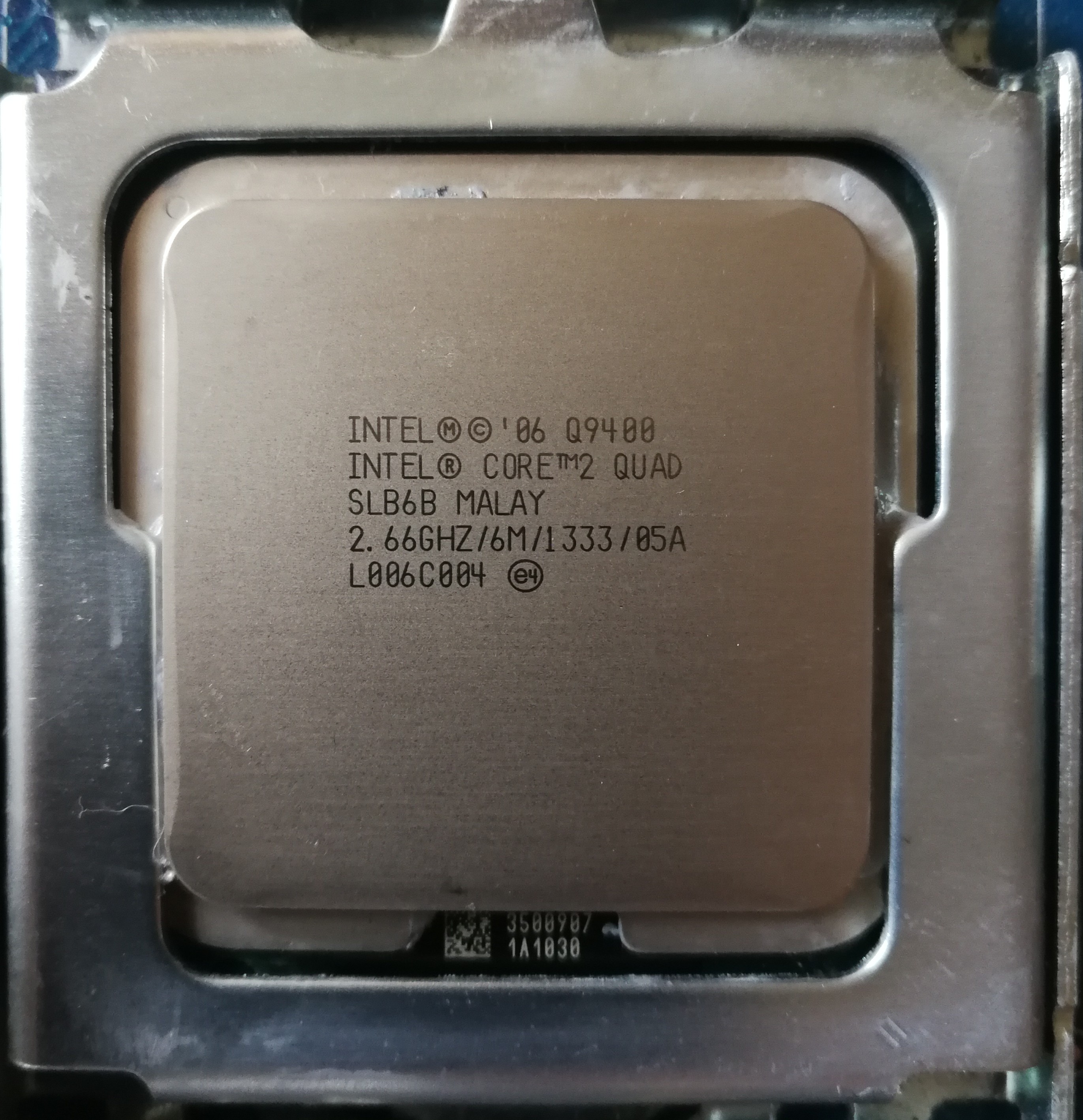 |
Intel Core 2 Quad Q9400 SLB6B - 2008 The L2 cache situation on Core 2 Quad was a little unusual. Q6x00 had 2x 4MB Q8x00 had 2x 2MB Q9x00 had 2x 3MB Q9x50 had 2x 6MB There's little more to say about Penryn which hasn't already been said, so an interesting diversion here is Dunnington. Take a Penryn 45 nm CPU core. Then two others. Put them all on the same die and you're now thinking "But the 1066 MT/s front side bus (FSB) will never handle three cores!" and it indeed didn't: Intel added an "uncore" to the die, which used Simple Direct Interface links to all three cores and ran out to the FSB itself. It also controlled a giant 16 MB L3 cache. The "uncore" was similar to (and by that, I mean a direct derivation of) Tulsa's on-die Cache Bridge Controller back in the NetBurst days. Like Tulsa's CBC, the uncore and L3 ran at half the core clock and directly connected to the FSB. Dunnington's L3 was implemented as four 4 MB blocks which were disabled to segment the product. All Dunnington Xeons were dual-die MCMs to give six total cores. Xeon E7420, for example, disabled half the L3 cache and one core per die, to give four total cores. The top of the line Xeon X7460 had all six cores enabled, ran at 2.66 GHz, full 16 MB cache, and a TDP of 130 watts. Dunnington's memory bandwidth constraint was extreme, however. x264 encoding needed twelve Dunnington cores over two sockets to beat AMD's quad-core K10. This drove Nehalem's on-die memory controller. Data below is, of course, for the quad core Core 2 Quad Penryn-cored Kentsfield, not Dunnington.
|
||||||||||||||||||||||||||||||||||||||||||||||||||||||||||||||||||||||||||||||||
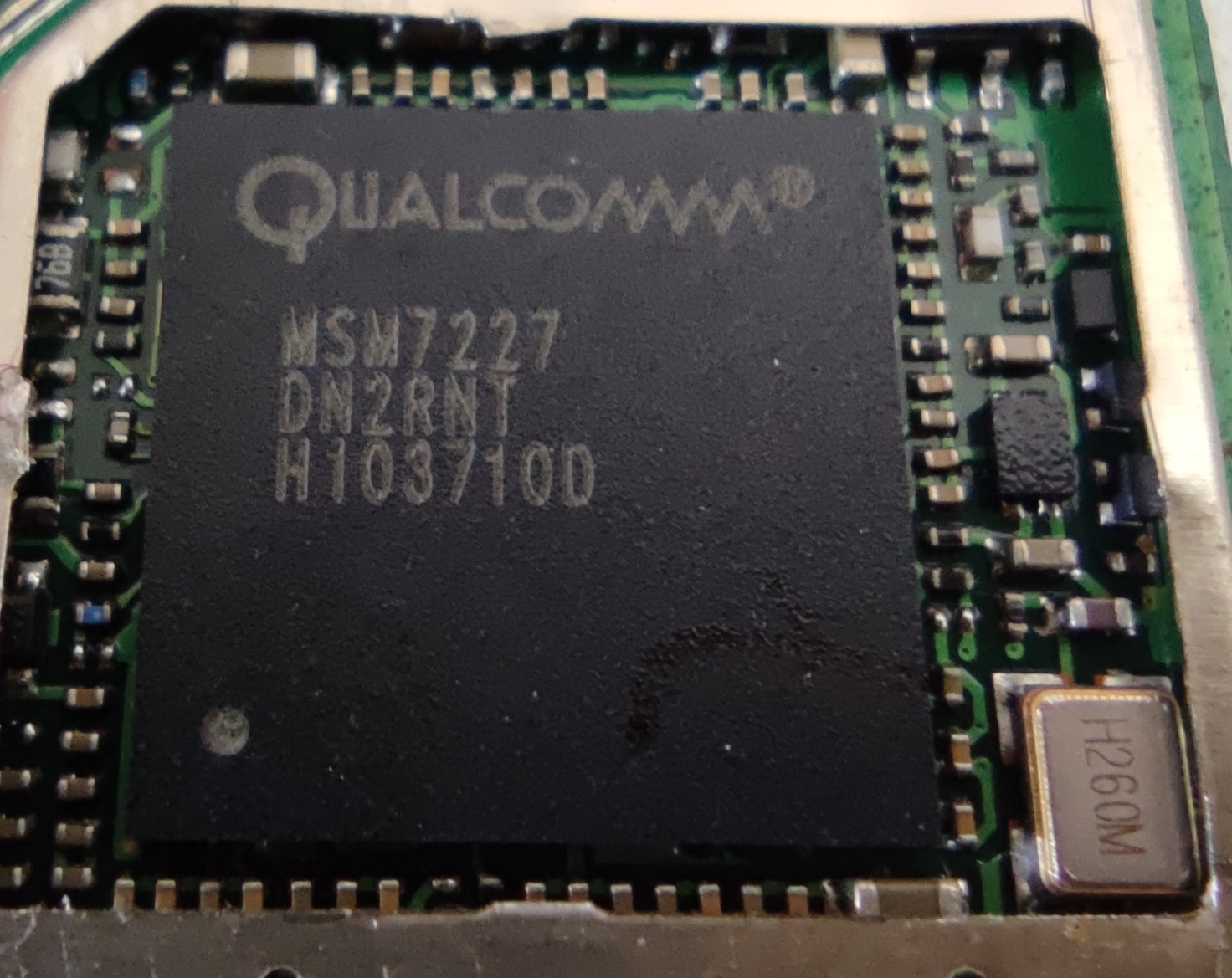 |
Qualcomm MSM7227 - 2008 The CPU in here, the ARM11, wasn't the biggest and best even for the time. ARM11 was announced as available by ARM in 2002, as the ARM1136. The 1156 (adds the Thumb2 16 bit architecture) and 1176 (adds security like NX) would follow. ARM11 was ARM's workhorse for embedded performance for some time, particularly when ARM9's chops just weren't meaty enough. The ARM11 core has a nominal 8 stages, can run in ARMv6 or Thumb mode, Thumb mode uses implied operands and 16 bit addressing, for low storage, low pincount, embedded designs. ARMv6 in general is designed for high instruction level parallelism, and indeed has significant parallelism within instructions. ARM11 introduces proper branch prediction (ARM9 did static "never taken" speculative execution) and has static "take if negative offset, never take if positive offset" prediction, so it prefers to branch backwards but not forwards. L1 cache is Harvard, 4-way set associative, and can be configured from 4 kB to 64 kB. Configured as the ARM1136EJ-S, this means the ARM11 core is about as basic as it comes. The "EJ" means it has Jazelle DBX and an enhanced Vector Floating Point unit (basic DSP SIMD), and the -S means it can do unaligned memory access. The CPU ran at 600 MHz, the GPU at 266 MHz, and the "baseband" at 400 MHz. Baseband was the modem and modem DSP for handling cellular telephony and data, in previous generations the entire hardware of a cellular telephone. In this generation, the two entire computers (baseband and application processor) had merged into the same silicon, but were architecturally still two distinct computer systems. As implemented in the MSM7227, it was given 2x 16 kB L1 caches and a 256 kB L2 cache and had a single 16 bit LPDDR memory controller able to run up to 166 MHz (1.33 GB/s). It had the Adreno 200 GPU at 266 MHz, QDSPv5 "Hexagon" (JPEG, MPEG, MP3/WMA assist) in its very earliest iteration, and an "image signal processor" (ISP) (hardware de-Bayer) able to handle a camera up to 8 megapixels. The GPU it its own little story. Qualcomm had no GPU other than a rasteriser in the earlier MSM7225 and MSM7625, but had recently bought Imageon from AMD. AMD had no intentions to go chasing the embedded market, and ATi had developed Imageon for exactly that. Qualcomm had already licensed the Imageon Z430, as Adreno 200, to deliver OpenGL ES 2.0 support. The ISP was also part of the Z430. When AMD bought ATI, Qualcomm cheekily bought Imageon from AMD. MSM7227 was everywhere in the Android 2.x generation, particularly at the entry level. It, almost single-handedly, drove Qualcomm's dominance in the Android space. Here we see it in a ZTE Blade, but it was also in devices such as the HTC Wildfire, the Samsung Galaxy Ace, and many, many, many others. Here in the ZTE Blade, it had 512 MB RAM, 512 MB ROM (juuuust enough) and came as standard with a 2 GB micro-SD. The screen, an 800x480 3.5" IPS at 240 PPI was by far the highlight of the device. This was the first wave of the smartphone revolution 2009-2012. It was when iOS (which had yet to take that name) and Android both became mature systems. Android 2.3 "Gingerbread" and iPhone OS 4.0 were finally sufficient to take on the entrenched featurephones and win. | ||||||||||||||||||||||||||||||||||||||||||||||||||||||||||||||||||||||||||||||||
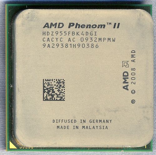 |
AMD Phenom II X4 955 Black Edition CACYC - 2009 When AMD launched the "K10" or "K8L" Phenom in 2007, it was found to have a rather embarrassing bug: The translation look-aside buffers could sometimes corrupt data. This TLB bug was blown out of all proportion (for most people it would and could never happen) but as far as CPU errata go, it was a pretty big deal. AMD fixed it by slaughtering performance of the Phenom chip, until the B3 revision which had fixed silicon. Without the "TLB fix", a Phenom was clock-for-clock about 10% faster than an Intel Core 2 Quad in some tests, 10% slower in others: In general, it was a wash. With the fix, it was as much as 15% slower across the board with the occasional dip to 30%. Additionally, the top speed grade on launch was 2.5 GHz and AMD's top end Phenom X4 9950 Black Edition only hit 2.6 GHz, and would overclock to around 2.8 only with extreme persuasion. Intel was firing with a 3.0 GHz Core 2 Quad at this time. While Phenom had somewhat of a per-clock advantage, Intel just had more clock and so the performance leadership remained in the blue corner. Unfortunately AMD was not firing against the older Core 2 Quads. AMD released Phenom II in 2009 to go against Intel's Nehalem chips, the first generation Core i5 and i7s. In summary, the L3 cache increased to 6 MB from 2 MB and the TLB bug was fixed. Also, per-core power management was disabled. Transistor count increased from 463 to 758 million, the chip size reduced from 283 mm² to 258 mm², L1 and L2 were made slightly smarter, prefetching was made more aggressive... Boring stuff, really. Clock for clock, AMD's new Phenom II was more or less identical to the older one... but it launched at 3.0 GHz and eventually reached 3.7 GHz as the Phenom II 985 Black Edition. Phenom II was really just a very minor update to the original Phenom, the main difference was that it had three times as much L3 cache and, due to the quite good 45 nm process and some critical path optimisation, could clock very high. Even original Phenom IIs on release were hitting 3.4 and 3.6 GHz. AMD's stepping code system didn't change for this era, but it did, of course, reset. Phenom II continued the stepping codes Phenom did, and it's not fully clear what these codes meant. "CACYC AC" was used for all manner of parts, but all based off the Deneb silicon. Some partial decoding was made: Second letter A means quad core or dual core silicon. C means six-core. Third letter C or higher means 45 nm "K10.1" based except when second letter is C. Fifth letter B means a 65 nm K10, C means a 45 nm K10.1, D or E mean a 45 nm six-core K10.1 The core stepping was different. For K10.1 on 45 nm, there were C2 (around 3.8 GHz max), C3 (3.8-4.0), D0/D1 (6-core) and while rumours of an E-code of an eight core were out there, nobody ever saw one. More on this near the bottom as a footnote. Later, a C3 stepping was released, which clocked much better and ran on less voltage. Most C2s topped out at 3.8 GHz no matter how hard they were pushed. C3s would hover around 4.0 GHz Phenom II disabled the original Phenom's per-core power states and instead ramped the entire four cores up and down as needed. This helped performance, but severely hurt power use. Phenom's on-die thermal sensor was also modified to only decline at certain maximum rate, so on returning to idle after a load, it would not show true temperature but a higher temperature. This was actually very good for watercoolers which would otherwise spin down their fans too rapidly to take coolant temperature down, but this side-effect was unintentional, as it was there to prevent fans from rapidly changing pitch. This is the earliest form of Tdie/Tctl and is a "temperature" measure intended to control fans. On AM4, Tdie/Tctl would allow the same cooler to handle all AM4 CPUs at any given TDP rating, as each CPU had a corrective "fudge factor" built in to correct for differences in Tdie (hence "Tctl" = Tcontrol). Phenom II was also available, soon after launch, on the AM3 platform, which ran on DDR3 memory. All Phenom IIs will work in AM2+ motherboards with DDR2 memory, as the CPU supports both. They'll even boot and run on an elderly AM2 motherboard, but the 125 W models will lock the multiplier to 4x (800 MHz) as AM2 lacks dual power planes. It was, per clock, about 5-20% faster than Phenom. Clock for clock, Nehalem (as Intel's Core i7 965), was as much as 50% faster than Phenom II, though in some tests - games especially - Phenom II was Core i7's equal (and sometimes sneaked a small win). Clock for clock, however, is a poor metric across different architectures, or we'd all still be using Pentium 4. Price is a better one, and Phenom II usually beat Nehalem at the same price. For the money, the Phenom II was quite acceptable and on the apex of the price/performance curve, right at the point where, if we go cheaper, the performance tanks and if we go faster, the price rockets. At launch, an AMD Phenom II X4 940 Black Edition would cost $240, a Core 2 Quad Q6600 was $190 and a Core i7 920 was $300 (and needed a $240 motherboard, while the Phenom II was happy with a $135 one). Of the three, AMD's was almost exactly half way between the uber-expensive i7 and the older Core 2 Quad. Should one have saved the money and gone with a Core 2 Quad? It depended. Mostly, the Core 2 Quad was about equal to the Phenom II. After a few releases, prices dropped. In 2009, it was Phenom II turf, all the performance of a fast Core 2 Quad Q9550 for cheaper, 8% cheaper in fact: The Phenom II 955 BE was introduced at £245, while a Core 2 Quad Q9550 was $266 - the AMD system used about 20% less power too. Add in that AMD's 790FX motherboards were around $40 cheaper than their Intel equivalents and you then had enough money left to bump the GPU a notch or two. If money wasn't an object, Intel's Core i7 could buy as much as 40% extra performance. By 2012, AMD was still selling the then-old Phenom II X4, including this 955 model, for the same price as Intel's Pentium G2120. The Phenom II was around 25% faster except in solely single threaded tasks. As of June 2014, the X4 955 Black Edition was going for about £55 on ebay. The king of the Phenom IIs, the X6 1100T BE, was over double that. The six core "Thuban" was really just Deneb with some minor revisions made and two more cores bolted on the side. It did have "turbo core" which was a really rough first generation implementation. The CPU would run three of its cores faster so long as it wasn't overloaded with power (125 W TDP) or temperature (95 celsius). This is because Windows, at the time, would do really dumb things with scheduling and would take a task off a 3.6 GHz core to give it to an 800 MHz powered down core. By 2014, however, it was time to put the K10.1 generation away. Being a new parent at the time, thart wasn't an option here! By 2015, they were definitely showing their age, but still quite useful even for moderate gaming. This Phenom II powered a primary gaming machine until February 2017, when it was really quite archaic, yet it performed quite well with a Radeon HD 7970 3 GB. It had given five years of reliable service and was bought as a pre-owned part to begin with. The manufacturing code on this chip is "0932" so it was manufactured in the 32nd week of 2009, and had therefore been retired from my service at the age of 8. It ran most of its life at 3816 MHz on a Gigabyte GA-990XA-UD3 motherboard, served by DDR3 memory clocked at 1413 MT/s. (HT bus 212 MHz, multiplier 18X - You sometimes wanted to bump the HT bus to get a slightly different RAM divisor) It was donated to a friend, where it lived out its remaining days, around another year of service.
|
||||||||||||||||||||||||||||||||||||||||||||||||||||||||||||||||||||||||||||||||
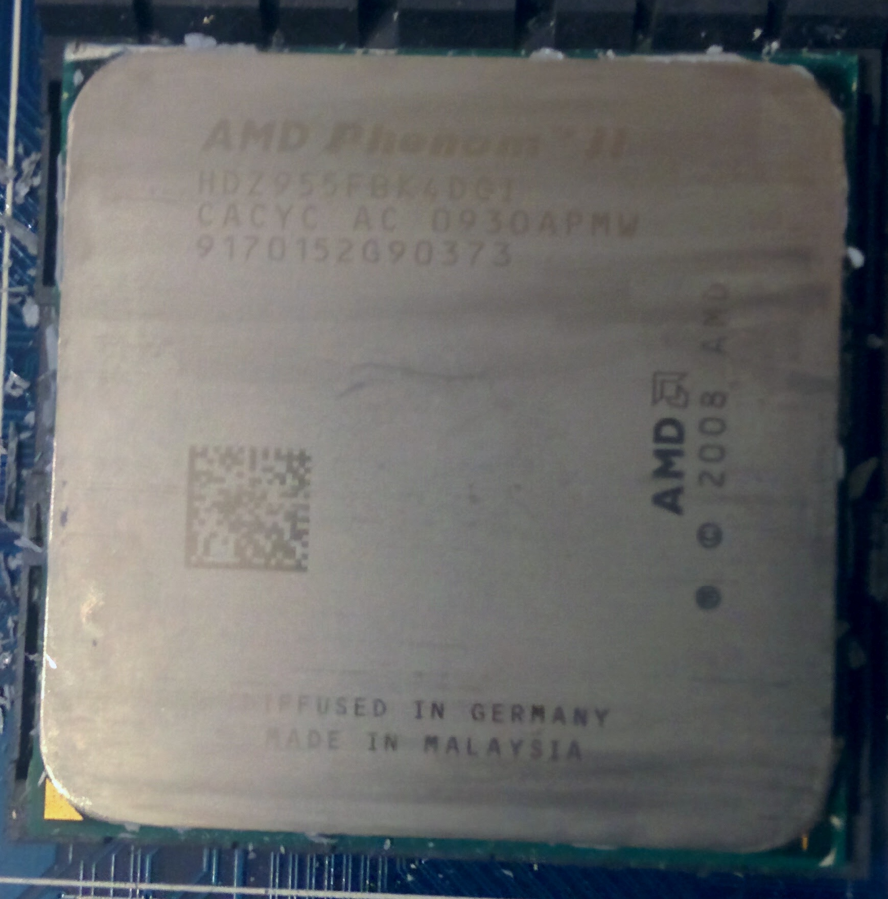 |
AMD Phenom II X4 955 Black Edition CACYC - 2009 Almost identical to the one above! It has the same CACYC code and the only real difference is the production code: This one is marked with 0930, the one above is 0932. They were made two weeks apart in 2009. One of the cool features of AMD's AGESA platform in K8 and K10 was "Clock Calibration". When AMD made K8, it could vary its clock on-die by 12.5% either way, but this was never really used. Windows was really bad at scheduling tasks relative to power states, even as Windows 7 (and up) had full control of both. Windows would see an idle core and schedule to it, meaning that core had to then come all the way out of a sleep state. AMD K10 increased this to each core able to vary clock individually and called it Advanced Clock Calibration, and again never really used it: It was for overclockers, so that weaker cores could be backed down and a higher peak clock reached on the good cores. However, it did have a bug, or at least an oversight. If we specified clock calibration on a CPU core which was sold disabled (e.g. the disabled one or two cores on a Phenom II X3 or X2, respectively), then the CPU's onboard firmware actually enabled that core! Maybe it worked. Maybe it didn't. It could be clocked down by up to -12.5% if it had a scaling defect, meaning that cheap X2 and X3 parts could have that bit of extra performance. The particulars are covered, we'll go into the history of this particular CPU. I bought it second-hand with an Asus Crosshair III Formula motherboard. The board turned out to be extremely flaky, and I got that refunded. No harm, no foul, but I still lacked a working motherboard. The AM2 board I had, the Gigabyte GA-MA69G-S3H, didn't implement dual power planes (AM2s didn't have to, although they could), so the Phenom II locked itself to 800 MHz. It worked, but was quite slow. HT bus overclocking got it up to about 1200 MHz, enough for basic use. I eventually got a proper AM3 board and, until February 2017, long after it should have been put out to pasture, it was my daily driver. As the Black Edition, this CPU has an unlocked multiplier so can be set to any clock the user desires. Most would end up between 3.6 and 3.8 GHz on air, this one is happy at around 3.7 GHz on air and 3.8 on water. To go higher requires cooling I plain do not have! At 3.8, it manages to hit 65C even with a Corsair H80 watercooler. High voltage (1.625V) tests at 4.0 GHz did boot, but hit almost 80C, FAR too hot. AMD's top bin was the 980 Black Edition, clocked at 3.7 GHz which almost universally would go no faster. It wasn't a great overclocker and 4 GHz was beyond the reach of most mortal men - They simply overheated rather than running into any silicon limit. Earlier Phenom IIs (such as the 940 intro model) would rarely pass 3.5 GHz. The C2 Deneb stepping generally ran hotter and didn't clock as well as the later C3 stepping. This is a C2, C3 appeared in November 2009. C3 also fixed issues with high speed RAM (4x 1333 MHz sticks could be iffy on C2) and ran at a lower supply voltage most of the time, so could be rated for 95 watts instead of 125 watts. C3 also implemented hardware C1E support. Most C3s would also overclock to around 4 GHz, but C2s ran out of puff around 3.8. Over time, the board or CPU or both started becoming a bit flaky. After changing from dual GPUs to a single GPU, the motherboard wouldn't come out of PCIe x8/x8 mode, so I tried resetting BIOS (clearing CMOS). This made one of the RAM slots stop working, and crash on boot (if it booted at all) with anything in that slot. Bizzare, I know. The RAM also wouldn't run right at 1333 MHz and had to be dropped down to 1067 MHz. Clearly, the board or chip weren't long for this world. This was in late 2015 or early 2016. I got another year out of it before BANG. It froze up while playing Kerbal Space Program and then refused to boot at all. I diagnosed it as a bad motherboard or CPU, given that they had been on their way out anyway, and got replacements out of an old Dell Optiplex 790. This turned out to be a Core i5 2500, which was actually a small upgrade from the Phenom II. To cut a long story short, the video card, a Radeon HD 7970, had died. The motherboard was flaky anyway, a RAM slot was unstable and the PCIe switch was locked into 8x/8x mode for no good reason, but it went back into use with a friend in Newcastle for around a year.
|
||||||||||||||||||||||||||||||||||||||||||||||||||||||||||||||||||||||||||||||||
  |
AMD Athlon II Neo N36L NAEGC AE - 2009 AMD's core codenames did not actually attach to silicon in this era. As the AMD Athlon II, this was Sargas. As Athlon II X2, it was Regor, as Phenom II Dual-Core Mobile, Turion II Dual-Core Mobile, V Series for Notebook PCs, and Turion II Neo Dual-Core Mobile, and Athlon II Dual-Core Mobile it was Champlain. As either Athlon II Neo or Turion II Neo for embedded, it was Geneva. It was obvious that AMD had got into a mess, and was using "common names" or "codenames" without any actual system. AMD was partiallycopying what Intel did with Merom and Penryn. Merom on the desktop was Conroe. Conroe mobile with some cache disabled was Merom-L. It wasn't the silicon which carried the name, but instead the intended market and featureset, so Champlain could be the same silicon as Deneb with cache disabled, but Regor couldn't be Deneb, but could be the same silicon as Champlain. To help straighten this out, we can sort them by die area in mm^2, which does not change between segments.
So this was named Geneva, but the actual silicon was the 117 mm^2 dual core "Regor" design without L3 cache and with 1024 kB L2 cache per core. This one has the product code AEN36LLAV23GM and is engraved with "AMD AthlonTM II Neo" and is mounted on an FC-BGA package for surface mounting. The particular codes here only ever seem to have been used in the HP ProLiant Microserver TL36, which is where this came from. AMD had got the 1024 kB L2 cache on Regor for free. The die size could only get so small before redesigning the HyperTransport and DDR2/3 memory controller, which fit around the outside, was needed. Deneb, Propus and Regor all use the same layouts for these, and the closest they can go together controls how small the die can get. Regor would have had blank space just under the memory controllers, almost exactly the size of an extra 512 kB L2 cache per core... so that's what AMD did. Blank silicon costs the same as featured silicon, so why not? The feature count below is taken from Tech Power Up's CPU database as of 2020/21 and almost certainly wrong. It gives the 117 mm^2 Regor 410 M while the 169 mm^2 Propus is given 300 M. These figures may be inaccurate or simply swapped. If we find better data, we will use it and remove this notice.
|
||||||||||||||||||||||||||||||||||||||||||||||||||||||||||||||||||||||||||||||||
 |
Intel Pentium E5400 SLGTK - 2009 Between Celeron (very low end) and Core 2 (enthusiast, gaming), sat Pentium. It was Intel's mainstream to low mainstream. It was for the boring office jobs, the point of sale systems (where this came from), the rising small form factor (SFF) PCs from the likes of Dell or HP. It was meant to be the journeyman of CPUs, to do anything reasonably well, to not be slow enough and crippled enough to embarrass itself, like Celeron did, and to not run fast enough to threaten the Core 2's price premium. Intel's MSRP on this was $67 in January 2009, it slotted into the well loved LGA 775, ran an 800 MHz FSB and was rated to 65 watts. This Pentium generation was also one of the first to support SpeedStep, which allowed the CPU to lower its clocks when idle. Core had supported it earlier, but the lower end always had it disabled. Even in laptops. C'mon Intel, seriously now? Wolfdale was the "tock" of Penryn's "tick" so was just a die shrink from 65 nm to 45 nm. All Pentiums (and Celerons) were Wolfdale-3M and even the fastest were rated at no more than 65 watts. This was not the fastest, far from it, and had a third of its L2 cache disabled. Wolfdale in this incarnation was a tiny 82 square millimetres die and ridiculously cheap to manufacture. The other variant of Wolfdale had 6 MB L2 cache and had SSE4.1 enabled (present, but almost always disabled on Wolfdale-3M. It seems Intel was experimenting with the possibility of dropping the "Celeron" and "Pentium" names, as CPU model numbers were remarkably consistent across the entire range. Celeron was the E3000 series, Pentium was E5000 and E6000, Core 2 Duo was E7000 and E8000. Only the OEM-only Pentium E2210 broke this trend, being essentially a Celeron with the wrong name. Of the Pentiums, E5000 told you it was on an 800 MHz bus, and E6000 gave it a 1066 MHz bus (it's really MT/s, the bus is quad-pumped AGTL+ introduced with Pentium4). A Pentium E6800, for $86, was a very cheap way to get a rather decent level of CPU performance (3.3 GHz) in late 2010. Wolfdale was an unhappy generation for Intel. Penryn was still available and selling well, so Intel had to undercut it slightly, and AMD's Phenom II X2 and X3 were outrunning Wolfdale. Nehalem was the new and cool, but had no dual core parts (Havendale was cancelled) and changed the socket. Finally, even the lowest Nehalem, the Core i5-750, was a 95 watt monster at $200. Wolfdale, like Westmere (the 32 nm shrink of Nehalem) was one of Intel's forgotten generations.
|
||||||||||||||||||||||||||||||||||||||||||||||||||||||||||||||||||||||||||||||||
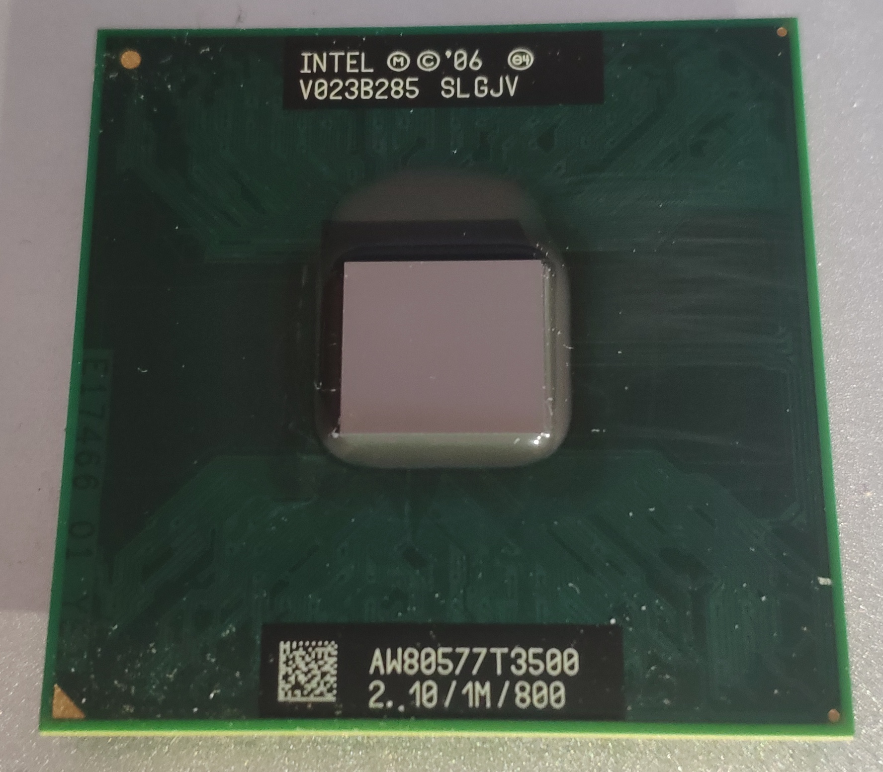 |
Intel Celeron T3500 SLGJV - 2010 The Penryn refresh series of Celerons for the mobile market were released in 2010 and 2011, when most Penryns were released in 2008. All Penryns ran on an 800 MHz FSB, but not all Celerons had two cores enabled. As a dual core CPU running at 2.1 GHz in 2010, this was quite reasonably performant, something few Celerons ever achieved. It didn't exactly go in the top laptops of the day, so would usually be found with 2 GB RAM in one slot, single channel. The T3500 had a TDP of 35 watts as its power management was mostly disabled. The very similar Core 2 Duo SL9600 (2.13 GHz, 6 MB cache) had a TDP of 17 watts and the identical Pentium T4300 (2.1 GHz, 1 MB cache) was 35 watts. All were based on the same 410 million feature Penryn-3M die.
|
||||||||||||||||||||||||||||||||||||||||||||||||||||||||||||||||||||||||||||||||
|
AMD Bulldozer - What The Hell Went Wrong?
If you put the specifications and design of Bulldozer between K10 and Zen, it is obviously a transitional step between them. Bulldozer had much better designed L2 and L3 caching subsystems, the "uncore" or NorthBridge was connected via a far faster bidirectional bus, L2 had two 128 bit write pathways and two 128 bit read pathways, together with a very fast 128 bit path to L1 cache. On seeing the caching architecture, where K10 had been limited, Bulldozer didn't just beat K10, it also beat Intel's fastest Sandy Bridge, and by an awful lot. L3 cache itself was the same as K10, but accessed in a way which made much more sense for a many-core design. Finally, AMD's DDR3 memory controller was superior to anything Intel had, and would ever have. 1st generation Bulldozer beat Haswell in DDR3 bandwidth tests. Bulldozer's codename wasn't randomly chosen, the design paradigm by Dirk Meyer was to to move an awful lot of data in and out of the cores. If the cores were relatively narrow, even modest instruction-level parallelism would be able to keep them completely full, and they could clock higher. The CPU front end, where instructions were decoded, decoupled the fetch/prefetch and branch units from the decoder and improved width from three ops per clock to four ops per clock. Branch prediction was massively improved from K10, adding a second level branch-target buffer and a hybrid "metapredictor" which combined local and global branch history. K10 had no local branch predictor at all. Bulldozer was still behind Sandy Bridge, but not by much. Out of order execution was also improved, and by a lot, from K10. K10 had retained K8's hybrid of a reorder buffer and rename register file (ROB/RRF), which was in turn copy/pasted almost unchanged from K7. Bulldozer used a physical register file (PRF) scheme, which was carried over to Zen. To all the world, Bulldozer looked like it would absolutely stomp K10. It was just better in every way. It even had power consumption modeling, which K10 lacked (Llano added it, it was not working well). Let's talk instead about how and why it failed so hard. At HotChips 2010 (link goes to the presentation) AMD presented Bulldozer, now pay attention to the L1 data cache here. 16kB?! The hell? Well, Llano gives us our first clue. Llano was a TeraScale 3 GPU and four Stars K10 cores on a 32 nm process. It lacked L3 cache, to fit the GPU, but nobody actually noticed that its L1D$ cache was dramatically different to Bulldozer, it wasn't just four times bigger! 32nm gave problems for 6T SRAM in read-modify-write cycles and in read timing. Simply put, 6T SRAM could not run at the clocks AMD wanted on the 32 nm process for Bulldozer. 8T SRAM could, but it was substantially larger on the die. By the time AMD learned this, the CPU had already been floorplanned and laid out. One can imagine the horror among AMD chip designers. They'd already cut the cache from 64 kB to 32 kB and, to make this thing ship at all, they had to shrink it to 16 kB. By now they would have realised that their "move an awful lot of data in and out" had just gone up in smoke. 16 kB wasn't enough for Intel's Banias in 2003, and that was a tiny, narrow, mobile design, it sported 32 kB I/D caches. This was the hill Bulldozer died on. Not only was the L1 data cache tiny, but it was also write-through. Chips and Cheese likened a write-through cache to skydiving without a parachute. It's much, much easier to do and a lot simpler, but you die. AMD added a write-coalescing cache so that any L1 data write isn't stuck waiting on glacially slow (relatively) L2 cache, but this marginally helped. Chips and Cheese compared that to skydiving with a very small parachute, and you'd wake up in hospital instead of not waking up at all, which is much better. That was AMD's problem. The L1 data cache, which was meant to be 64 kB, couldn't actually fit on the die and would intrude over to the other module. In 2009, AMD presented it as being 32 kB, then by HotChips 2010, it was showing only 16 kB. People who knew their stuff immediately started sounding alarm bells. Bulldozer was going to be extremely problematic if it only had 16 kB L1D$! Bulldozer's L2 cache was far superior to K10, and even better than Sandy Bridge, while L3 cache was not as impressive: It didn't need to be with L2 cache being so good. Bulldozer's branch prediction, decode width, despatch width, memory controller performance, these were all easily enough to do battle with Sandy Bridge. Everything about Bulldozer was a generation (if not two generations) ahead of K10, and either just behind Sandy Bridge, on its level, or even superior to it... Everything except that absolutely dismal L1 data cache, and that single mistake ruined AMD's entire CPU lineup from 2011 to the release of Zen in 2017. It cost AMD its fabs, it cost AMD its reputation, it cost AMD over a billion dollars in losses. Only the remarkable success of the GCN graphics IP and its selection for both Microsoft and Sony's consoles seems to have kept AMD afloat. It's tempting to wonder "What if?" here. What if AMD had not fucked up so massively? What if the L1$ had actually fit on the die, if the 6T SRAM had worked, the problems surmounted, and Bulldozer had shipped with 32 kB L1D$? We'd have been looking at a launch performance roughly the same as Sandy Bridge. It'd have had a single thread performance disadvantage, a power disadvantage, but a large clock speed advantage. It'd be like Intel's i9 14900K against AMD's R7 7800X3D, the i9 has all the same disadvantages a 32k L1 Bulldozer would have had, and the 7800X3D has all the advantages Sandy Bridge had against it. Intel now, like AMD would have done then (and AMD actually did back then!), is throwing power at the problem, needing 250 watts to keep up with a 95 watt competitor. AMD would have had the financial status to be able to iterate the Bulldozer design (the basic core design was never improved!) as Intel did with Sandy Bridge to Haswell. The low hanging fruit here are the ones the Zen designers picked up, they'd have been done earlier and would be more mature by now. Clustered multiprocessing (CMP) was not, and is not, a bad idea. By the time Bulldozer would have been threatened by Intel development - Skylake - everything on the PC which was performance sensitive was multithreaded, even games, and CMP is far better than SMT at extracting more multithreaded performance: A CMP module can run two threads faster and more efficiently than a single SMT core. We can see this from data which could fit in the tiny L1 cache of Bulldozer running two threads, it would usually beat Sandy Bridge, and not marginally either. This is, however, not what happened, and AMD was taught a very harsh lesson. Dirk Meyer was ousted as CEO in 2011 (this was coming anyway) and he was the key proponent of CMP. Lisa Su (who is actually Nvidia CEO Jen-Tsun Huang's cousin!) is given credit for "turning AMD around" after she joined in 2014, but the salvation of AMD had actually been Rory Read, CEO from 2011 to 2014, who developed the strategy of making the best of a bad situation and pushing semi-custom designs to the console makers to earn the cash needed to redesign the Bulldozer architecture into something that would work better - Zen. Read lowered costs, stripped out business units he felt were irrelevant, restructured AMD's debt, and diversified the sales markets aggressively. Read had seen that AMD's Bobcat CPU architecture was the key ingredient which would make semi-custom console APUs fit better than any other architecture. By the time Rory Read left AMD for a position at Dell, overseeing the merger of EMC into Dell, AMD had already turned the corner and was in non-GAAP profitability. Lisa Su got to reap the harvest Rory Read had sown. | |||||||||||||||||||||||||||||||||||||||||||||||||||||||||||||||||||||||||||||||||
 |
Intel Core i5 2500 SR00T - 2011 This Sandy Bridge HE-4 processor was Intel's mainstream along with the i5 2300 in 2011-12. Sandy Bridge's launch was... Uneasy. Intel had forced everyone else out of the chipset market by strong-arming, patent lawsuits, and closing the platform down by not documenting it. The last third party chipset vendor was Nvidia, still barely clinging on at the end of the LGA775 era, but had already failed to negotiate a license for Intel's "Direct Media Interface" (DMI) new bus. It's worth noting what DMI was: It was PCIe 1.1 x4 with an authentication protocol to disallow non-Intel chipsets. DMI 2 was... you guessed it... PCIe 2.0 x4. You'll never guess what DMI 3 was! At this point, Intel became extremely abusive in the market. Direct Media Interface 2 was the replacement of Direct Media Interface, which Intel had used as an interconnect between MCH/GCH (Northbridge) and PCH (Southbridge) for many years. With memory and graphics now on the CPU, MCH/GCH did not exist and so the CPU connected directly to the PCH. DMI 2 was far more similar to DMI than Intel would admit, and its changes seemed to be purely to make it eligible for new patents. Intel then did two abusive things: 1. Intel refused to allow third party chipsets 2. Intel refused to allow backwards or forwards compatibility When Ivy Bridge came along, The C600 Patsburg chipset was artificially forbidden from working with Ivy Bridge, despite it being the exact same silicon as Intel's X79... which DID support Ivy Bridge! Intel also tended to change the sockets by a pin or two to make the CPUs physically incompatible, even if they were electrically compatible. Sandy Bridge all the way to Haswell used DMI 2.0. Then, Skylake all the way to Coffee Lake (and maybe beyond) used DMI 3.0, despite each generation having a new socket and a new chipset. Why? Well, Intel used older fab processes for chipsets and it was a captive audience. What else are you going to use? SiS, VIA, Nvidia, ATI, SuperMicro, ServerWorks, everyone else had been forced out of the market. This was very good for profit. Intel's Cougar Point chipset (marketed as P67, H67, 6-series, Q65, etc., all the same chip) had a severe SATA controller issue. Intel didn't recall anything as this was unthinkable, it would leave Intel without the ability to sell any Sandy Bridge CPUs. The issue was that the SATA ports would degrade over time, slowly reducing throughput. Intel quoted a 6% performance drop over three years, but given Intel's previous statements on flaws, that was probably extremely optimistic. A single transistor was being overdriven, enough to degrade much more rapidly than intended and cause a steadily rising SATA error rate. X79/C600's SAS backplane and SATA ports were not affected. In time, the issues were fixed and Sandy Bridge was an exceptional performer. Indeed, Sandy Bridge is rightly regarded as one of the all-time greats. Its predecessor, Nehalem, ran hot, didn't clock well and AMD's Phenom II was able to keep up by throwing clock at the problem: A Core i7 920 ran at 2.67 GHz, while a Phenom II X4 980 ran at 3.7 GHz. The i7 920 would be around 10-30% faster. Running at 3.0 to 3.4 GHz, the top end Sandy Bridge processors were 10-30% faster still. Announced at Intel Developer Forum (IDF) 2010, even Intel seemed to be taken aback at just how powerful Sandy Bridge was. Sandy Bridge, in some rare cases, doubled the speed of Nehalem. That level of performance leap had last been seen with AMD's Athlon in 1999. Even Core 2 hadn't jumped ahead by that far. The processor graphics, now on the CPU die, was immensely improved over Intel's previous chipset graphics. It wasn't just some stripped back basic video solution intended to just make sure basic 3D and video decoding worked, it was finally serious hardware. It benefited from having direct access to L3 cache and greatly improved media processing ability. The GPU ISA was tightly coupled with DirectX 10, like a high performance gaming GPU was. At the same clock, it was at least twice as fast as the previous generation. In all, Sandy Bridge was so far ahead of Nehalem that it took until Kaby Lake in 2017 for Intel's lineup to progress as far from Sandy Bridge as Sandy Bridge had from Nehalem, its immediate predecessor. This particular unit is the Sandy Bridge HE-4 processor, which has four HyperThread(tm) (SMT) cores, 12 GPU execution units (EUs) and 8 MB of L3 cache. Intel is Intel, however, and a good deal of that is disabled. In the i5 2500, 2 MB of L3 cache is disabled, half the GPU (6 EUs) are turned off, HyperThreading is turned off and the CPU is clock locked to 3.3 GHz with opportunistic boost to 3.7 (turbo table is 3.7, 3.6, 3.5, 3.4). Of the 1.16 billion transistors on the chip, about two thirds are enabled. Notably, Intel split the GPU provision into "Graphics Tier 1" and "Graphics Tier 2", or GT1 and GT2. The i5 2500 was GT1, so had only six of its GPU units enabled of the twelve on die. The GPU was also de-clocked, but all Intel Sandy and Ivy Bridge GPUs weren't actually clock locked and could be freely adjusted by Intel's own tweaking utility. This is known as "configurability" and was a major design goal for Sandy Bridge. The quad core, 8MB L3, 12 EU had "chop zones" where the mask could be simply ended at that point. Chop zones allowed for the GPU to be chopped completely off or in half, for the IA cores to be chopped in half from 4 to 2 and for L3 cache to be chopped to 1.5 MB. L3 was in 512 kB blocks per core, and usually each core had 4 blocks. Mixing and matching these chopped zones allowed for multiple dies to be produced from the same design. Intel built three in the client space: 1: 4 CPU Cores, 2 MB/core (8 MB), GPU with 12 EUs. 1.16 billion transistors in 216 mm² 2: 2 CPU Cores, 2 MB/core (4 MB), GPU with 12 EUs. 624 million transistors in 149 mm² 3: 2 CPU Cores, 1.5 MB/core (3 MB), GPU with 6 EUs. 504 million transistors in 131 mm² As with all Intel products, it is heavily fusible, a post-production configuration. L3 cache was made of "slices", of which each enabled core had 2 MB worth. It could be fused off in 512 kB segments. Each fusible segment was 2 associative sets, so dropping from 2 MB to 1.5 MB dropped associativity from 16 way to 12 way. All slices had to have the same amount of L3, but not necessarily the same physical segments enabled, allowing Intel to fuse off defects as well as reduce performance for lower grades. Other fusible features were HyperThreading, virtualisation, multiplier lock, Turbo Boost functionality, individual cores, whether L3 (or L2) cache could even be used at all, whether the onboard GPU could use 12 or 6 EUs, and more. For $11 (on release) more, you could get the clock unlocked as the i5 2500K, which would often overclock as far as 4.4 GHz easily. Such a chip would still be competitive years later. By 2019, quite a lot of i5 2500K and i7 2600K processors running north of 4 GHz were still in daily use. Some approached and even hit 5.0 GHz with exotic cooling and modified motherboards. Sandy Bridge was one of the all-time greats produced by Intel, so much so that Intel produced 17 different variations on this same HE-4 silicon in the "Core i" line and several variants in the Xeon E5 (e.g E5-2637) and all the Xeon E3 line. HE-4 also powered all of Intel's quad core mobile chips of this era, where it normally ran between 2.0 and 2.5 GHz. The GPU in Sandy Bridge was very ambitious, at least by Intel's standards. It had long been held that a discrete GPU, no matter how weak, would always be greatly superior to any integrated graphics processor (IGP). With 6 EUs at a peak of 1100 MHz, this i5 2500 was between 50% and 66% of the performance of a contemporary Radeon HD 5450. This was epic. It was within spitting distance of a discrete GPU. A tremendously weak entry level GPU, but still a discrete GPU! The 12 EU part could deliver similar performance to the HD 5450, but was only available on few, seemingly random, i3, i5 and i7 parts. Sandy Bridge was so effective that, six years later in 2017, the i5 2500 (not the unlocked "2500K"!) was still selling for around £50 on eBay. The i7 2600, a cheap and moderate upgrade, was just over double that.
|
||||||||||||||||||||||||||||||||||||||||||||||||||||||||||||||||||||||||||||||||
|
Qualcomm Snapdragon 800 - 2012 Not that visible, as it was mounted package-on-package under a Samsung LPDDR3 RAM package here, it was nevertheless the top of the line at the end of 2012. Qualcomm had packed in four Krait 400 ARMv7 cores, their Adreno 330 GPU, the Hexagon DSP, dual image signal processors (basically hardware de-Bayer for cameras) and I/O support for eMMC5.0, SATA3, SD UHS-I. The CPUs clocked as high as 2.3 GHz, but most designs kept them between 1.8 and 2.0. The Krait CPU cores are synthesised with 32 kB of split L1 cache (16d$/16i$) and a shared 2 MB L2 cache. Memory access is via a fast, for the time, 64 bit LPDDR3-1600 bus, delivering up to 12.8 GB/s. The performance of Snapdragon 800 came from its four ARM Cortex A15-alike CPUs and its fabrication on TSMC's HPM (high performance mobile) as it was much more similar to the older Snapdragon 600 than Qualcomm was ever going to admit. The Krait 400 differed from Krait 300 by having larger L2 cache. Other changes were support for faster LPDDR3 (800 vs 533 MHz) and the GPU ran at the same clocks (450 MHz) but increased the SIMD-16 execution unit provision from four units to six. In all, Snapdragon 800 was extremely similar to the earlier Snapdragon 600 (which was renamed from Snapdragon S4) but turned up to 11. Qualcomm knew when it had a winner, as the later Snapdragon 801 was the exact same thing, even down to part numbers, clocked higher thanks to TSMC's 28 HPM process maturing excellently. | |||||||||||||||||||||||||||||||||||||||||||||||||||||||||||||||||||||||||||||||||
|
Intel Core i5 3470 SR0T8 - 2012 Ivy Bridge was the 22nm shrink of the 32nm Sandy Bridge. The on-die GPU was updated, but the CPU was not. This Ivy Bridge was of stepping revision N0, identifiying it as an Ivy Bridge HM-4, a 133 mm^2 die and 1.008 billion features. It had 4 cores and 6 GPU execution units (EUs). L3 cache was 6 MB, although some sources claim it was 8 MB and disabled to 6 MB like Sandy Bridge was: I find this unlikely, given that the Ivy Bridge based mainstream quad-core had fewer die features (1.01bn vs 1.16bn) than the Sandy Bridge. The 133 mm^2 die had a MSRP of $184. Intel's operating margin at this point was around 70% for CPU products, which shows: AMD's Cape Verde GPU was on a similar 28 nm process, at a similar 123 mm^2 size, had a significantly denser and more complex layout at 1.5 billion features, and sold in video cards priced at half the price of the i5 3470 as just a CPU. Ivy Bridge in general was a bit of a disappointment. The leading Core i7 3770K was launched in mid-2012 and replaced the Sandy Bridge Core i7 2700K, which came a little later in Sandy Bridge's life. It had the same base clock, the same turbo clock, and only added DDR3-1600 support, which Sandy was doing anyway on some motherboards. The "recommended customer price" was also the same. 3770K also had a significantly worse GPU due to most of it being disabled! Intel made much of Ivy Bridge's superior GPU, and even claimed that AAA titles would be playable at medium to high settings, at 1280x720. Not on the 6 execution units of the i5 3470 they weren't. With "Intel HD Graphics 2500", Ivy Bridge had 6 execution units, each of which had 8 shader cores, for a total of 48 "GPU-style cores". It clocked to a maximum of 1150 MHz, delivering 110.4 GFLOPS of pixel crunching power. This compared moderately well with a Radeon HD 5450 from two years before. The much more powerful Intel HD Graphics 4000 had 16 execution units, so 128 shader cores, and was allowed to clock to 1300 MHz, giving 332.8 GFLOPS, three times the performance. This was indeed able to run some games acceptably. So, knowing we were on the "GT1" level of performance, I tried a very graphically light game, Stardew Valley, at 1280x720. It was playable, but juddery at times, particularly when the weather became rainy, or a screen effect came on. A regular I've used for years, Aquamark 3, gave a score of 65,000. Oddly, the CPU score was very low and the GPU score very high - Higher than a GTX 680. I can only conclude that the 2003-vintage Aquamark 3 has finally ended its usefulness. Most lower Ivy Bridge parts boosted clocks by around 100-200 MHz for the same price as their Sandy Bridge predecessors and they all used much less power to reach those clocks. When pushed hard, however, Ivy Bridge tended to overheat at lower clocks than Sandy Bridge did. While a Core i7 2600K would quite readily hit 4.4 GHz on a decent cooler with temperatures below 70C, a Core i7 3770K would usually run out of steam at 4.2 GHz, despite a lower package power, and it'd hit 80-90C. Intel had changed from high quality, expensive solder thermal junctions to cheap thermal paste. Just what you want on your $330 CPU. It shows again that, in tech, price does not always (or usually) relate to quality. 
Note on delidding: Do not try it on a CPU with a soldered IHS. It almost certainly will damage the die. Delidding Ivy Bridge was very easy, a razor blade could do it, and reduce temperatures by around 10C. Of course the hotter it ran the more benefit delidding would get. As the i5-3470, it had a maximum multiplier of 36, to give a peak clock of 3.6 GHz, and a base clock of 3.2 GHz. HyperThreading(tm) was disabled, and the thermal design power (TDP) was 77 watts. This particular part replaced an i5 2500, which was almost identical. The i5 2500 had a 3.3 GHz base clock and a 3.7 GHz peak clock, but in reality it hovered around 3.5 GHz. The 2500 was rated to 95 watt thermal design power, although I had trouble getting more than 70 watts out of it, even in utterly unreasonable stress tests. The same Prime95 AVX small-FFT test that got 76 watts out of a Core i5 2500 could manage only 43 watts out of this i5 3470. The Sandy Bridge has 100 MHz more clock, but that's about it. As stated, the Core i5-2500 had a 100 MHz clock advantage, as well as a faster onboard GPU, but in practice the Ivy Bridge also allowed DDR3-1600 over the 1333 on the Sandy Bridge, so improving maximum memory bandwidth from 21 GB/s to 25.6 GB/s. It was a wash. There was less than 5% either way between the two CPUs. When the i5 3470 was new, it was best to spend £15 more and get an i5 3570K. It ran 200 MHz faster across the board and used the silicon with much more onboard GPU. The turbo table for this was 36, 36, 35, 34.
|
||||||||||||||||||||||||||||||||||||||||||||||||||||||||||||||||||||||||||||||||
|
Intel TurboBoost
As the name suggests, this uses a turbine to... No it doesn't. No turbine is involved. Just marketing professionals who don't understand technical terminology. Early versions of TurboBoost used a turbo-table, such as the 36, 36, 35, 34 in the Core i5 3470 above. The Intel driver adjusted the CPU's global multiplier based on how much CPU load it measured. The nomenclature was "1 core, 2 core, 3 core, 4 core" and so on, so the 3470 would boost to a 36 multiplier with a 1 or 2 core workload, but only 34 with an all-core workload. The TurboBoost would drop down if the platform limits (temperature, current, power, etc.) were met. PL2 was, on most setups, essentially unlimited power and more than the CPU would ever use in normal (even all-core) operation, but this expired after around a minute or less (PL2 time limit was "tau"), and PL1 applied, which would cause power throttling. This was TurboBoost 2.0, as seen in Sandy Bridge and Ivy Bridge. It was also taken forward to Haswell and Broadwell. Skylake introduced "TurboBoost Max 3.0", which was a superset of TurboBoost 2.0 (and was disabled in most of the lineup, because Intel gotta Intel). Turbo 3.0 (for brevity) introduced "short-boost" and the boost behaviour from 2.0 became "long-boost", as well as configurable TDP implemented by the same dynamic voltage/frequency scaling system. The boost times were controlled by a parameter Intel branded "tau", which was immediately abused by motherboard manufacturers to make their boards short-boost pretty much indefinitely, making Intel CPUs far more power hungry than they were designed to be. This is controlled by a number of variables, which we'll use Intel's names for. PL1 is power limit 1, the limit the CPU is allowed to maintain for long periods. This should be set to equal to the cooling capacity of the system or only slightly above it. PL1 is supposed to be what the VRMs can deliver indefinitely and the cooling system can handle indefinitely. PL2 is the short-duration power limit and usually very, very high, maybe double PL1. This is only a few seconds. Intel usually specifies this between 8 and 100 seconds (40 seconds was typical), but it does vary based on the processor type. PL2 is meant to be the thermally limited VRM power, related to AMD's "Thermal Design Current". On enthusiast motherboards the VRMs are usually extremely well cooled and highly provisioned, able to sustain powers well over 200 watts indefinitely, so this doesn't actually make sense there. There are also PL3 and PL4, which are more for motherboard manufacturers and OEMs to ensure the CPU doesn't exceed the limitations imposed by VRMs. The CPU will only use PL3 or PL4 for milliseconds. PL3 is used in mobile sytems, it is the power source limit, such as the battery's maximum discharge rate. PL4 represents power delivery limits, so the maximum the VRMs can deliver without damage. PL3/4 are analogous to AMD's "Electrical Design Current" and represent what AMD calls "infrastructure limits". |
|||||||||||||||||||||||||||||||||||||||||||||||||||||||||||||||||||||||||||||||||
|
Intel Core i5 3570K SR0PM - 2012 The i5-3570K replaced the i5-2500K in the market as a mainstream/high end overclockable CPU. Overclockers were expecting great things from the 22 nm shrink of the very well clocking Sandy Bridge. An i5-2500K would usually get to 4.0 GHz and more wasn't unheard of. Single core turbo on a i7 2600K was well understood to be easily over 4.5 GHz and maybe approaching 5.0 GHz on a good sample. Ivy Bridge ran hot. A 3570K would run between 4.2 and 4.3 all day, but keeping it cool was a problem. Intel had changed the integrated heatspreader to being attached to the die with cheap thermal interface material instead of metal solder of Sandy Bridge, Nehalem, and all previous processors as far back as Willamette! With a Corsair H80 closed loop liquid cooler, this 3570K hit 92C at 4.2 GHz all-core load and that was considered good! You'd think i5-3570K was the "overclockable version" of i5-3570, and you'd be wrong. i5-3570 was much less popular than i5-3470, and was made of the same HM-4 silicon as 3470. 3570K was made of the HE-4 silicon....We'd better explain that. HE-4: 4 CPU Cores, 4/core (8 MiB), GPU with 16 EUs. 1.4 billion transistors in 160 mm² HM-4: 4 CPU Cores, 3/core (6 MiB), GPU with 6 EUs. 1.0 billion transistors in 133 mm² H-2: 2 CPU Cores, 4/core (4 MiB), GPU with 16 EUs. 0.83 billion transistors in 118 mm² M-2: 2 CPU Cores, 3/core (3 MiB), GPU with 6 EUs. 0.63 billion transistors in 94 mm² The "M" signified it was designed for power efficiency ahead of scalability, today we call this "low-power" or "mobile". Ivy Bridge had 2 core and 4 core levels, and each of those has 6 GPU and 16 GPU levels, for four total die models. M-2 was 2/6, H-2 was 2/16, HM-4 was 4/6 and HE-4 was 4/16. 3570K had the 16 execution unit GPU enabled, but 2 MB of the 8 MB L3 cache was disabled and SMT was disabled. Bizzarely, the H-2 silicon was only ever used in Core i3-3245 and Core i3-3225 on the desktop, but was very widely used mobile, as it was very effective with its larger GPU. The turbo table for this 3570K was 38, 38, 37, 36. This was my main desktop until late 2020, when a Ryzen 5 5600X replaced it and became my first all-new personal system build for over fifteen years. Having kids will do that to you. It then languished in storage until July 2023, when it took over duties of running this server from a dual Xeon E5 2640, which it was roughly a third of the performance of and had one quarter of the RAM. Being way too old for its job led to a replacement by a Xeon E5-2640v3 in 2024. The Xeons had 32,400 core-MHz (2,700 x 12), while the i5 3570K had only 14,400 (3,600 x 4), and both were of Sandy Bridge cores (Ivy Bridge didn't change the CPU core). In pure MHz, the Xeons had a 2.25x advantage. This performance disparity was fairly linear in threaded workloads. Cinebench R20 went from 2,708 with the Xeons to just 1,027 with the 3570K, a ratio of 2.64x. This also tells us how little Cinebench cares for L3 cache, HyperThreading, or RAM bandwidth, which the Xeons dramatically outgunned the little Ivy Bridge in and, yet, squeezed only a little more IPC in Cinebench R23: 0.0836 points per MHz on the Xeons, 0.0713 points per MHz on the 3570K. Why, then, would I do such a thing? The Xeons had no GPU (a small Radeon HD 5450 was used for video output, when that was needed) and the major role of the server had become my home CCTV system, which was entirely software H.264 encoding and decoding on the Xeons. Of course they had more than enough power for it, but they then ran at around 160 watts from the wall. The 3570K could do that in its GPU hardware, cutting power consumption by around half. The only other major use was as a storage server, and the Xeons in their Dell Precision T5600 chassis could not physically hold enough HDDs, so the PERC H310 SAS controller was flashed to IT mode and went with the role into a nice big late-2000s Cooler Master case, an original CM690. We don't cover cases here, but the CM690 was a fine example of its era. Four optical drive (5.25") bays, six 3.5" bays, no 2.5" bays at all (they were for laptops exclusively) but very little in the way of airflow. Intakes were one front fan (a slow 140 mm) and a mounting for one 120/140 mm fan intaking on the bottom. Exhaust was a single rear 120/140 mm fan. By today's standards, we'd call it an "oven" but back then this was quite a lot of airflow. A heavily loaded high end gaming PC would rarely use more than 350 watts. My CM690 came from a Core 2 Quad Q6600 + GTX 8800GTS + 8 GB DDR2-800, which had been retired and I bought it for the case in 2020.The i5-3570K in the CM690 was later replaced by a Xeon E5-2640v3, which also had no GPU, but a Radeon HD 5770 handled that. As of 2024, a CPU around this performance was the under the cut-off of what a useful PC could have. I'd begun rejecting Ivy Bridge for refurbishment and was using only Haswell (even then, only the DDR4-supporting Xeons, since DDR4 memory was very highly available. 16 GB DDR3 was a crapshoot, and 16 GB was the minimum acceptable) or higher. By 2025, that'll probably move to Skylake with the EOL of Windows 10.
|
||||||||||||||||||||||||||||||||||||||||||||||||||||||||||||||||||||||||||||||||
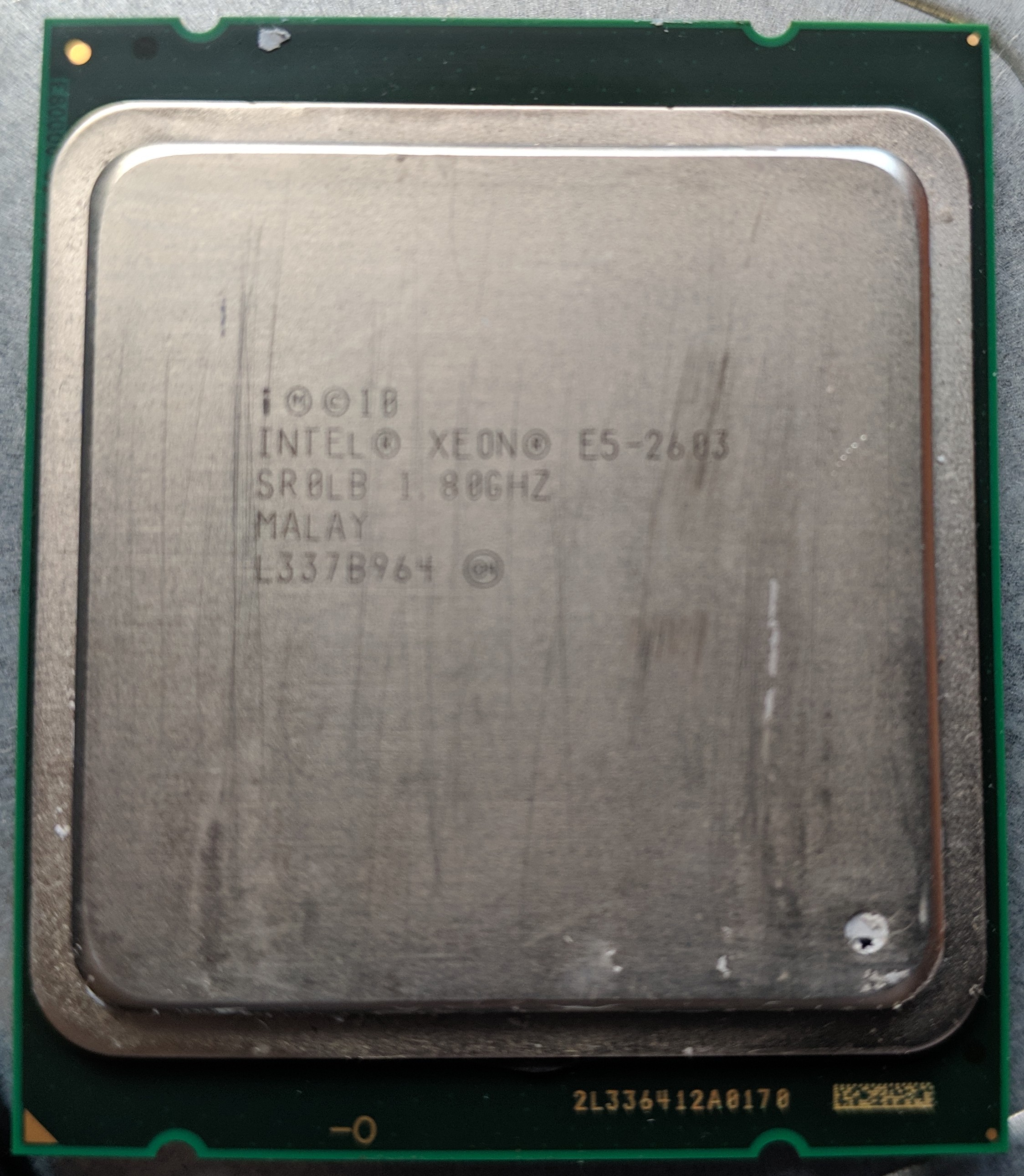
|
Intel Xeon E5-2603 SR0LB - 2012 In 2012, Intel released the Sandy Bridge-E processors and differentiated them by socket. 1P LGA 2011 got "E", 1P/2P LGA 1356 got "EN" and 1P/2P/4P LGA 2011 got Sandy Bridge-EP. This one is an EP, meaning it supports Direct Media Interface (DMI, the connect to the chipset), quad-channel memory, and 2x Quick Path Interconnect (QPI, inter-processor communication). Sandy Bridge-E also added official DDR3-1600 support. The main change to the "E" series was that they were made up of "slices". Each slice was two cores and 5 MB of L3 cache. L2 cache was a static 256 kB per core. On the die, a slice was a core above, 2.5 MB of L3, crossing the middle of the die, then another 2.5 MB L3, then the core at the bottom. A ring bus went through all the L3 caches, as can be seen. 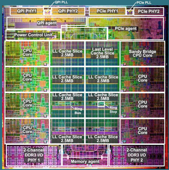 Image copyright Intel At best here, then, we have eight cores, 20 MB L3 cache, four DDR3 channels, two QPI links. The diagram is the "four slice" design. These have the "C1" or "C2" stepping code. Our part here, with S-Spec of SR0LB, was not C1 or C2: It was M1, meaning it was a two-slice die. The Xeon E5-2603 was not the best. In fact, it was the worst, or at least the worst with four cores. It used either binned (disabled) 8-core chips (these are C1 or C2 and very rare to see in four core configuration), or the smaller Sandy Bridge-E which had only two slices on the silicon. It was limited to 1.8 GHz, TurboBoost was disabled, HyperThreading was disabled, QPI was limited to 6.4 GT/s (7.2 and 8.0 were the usual speeds) and the memory interface had 1333 and 1600 speeds disabled. It was, however, very cheap, just $198 on release. This one came in a Dell Precision T5600 workstation which had been configured more or less to its minimum spec. Of the two processors supported, one of them plain wasn't fitted at all, the one that was was this slow Xeon. It did have 16 GB RAM, an awful lot for the time, which was both registered and ECC protected.
|
||||||||||||||||||||||||||||||||||||||||||||||||||||||||||||||||||||||||||||||||
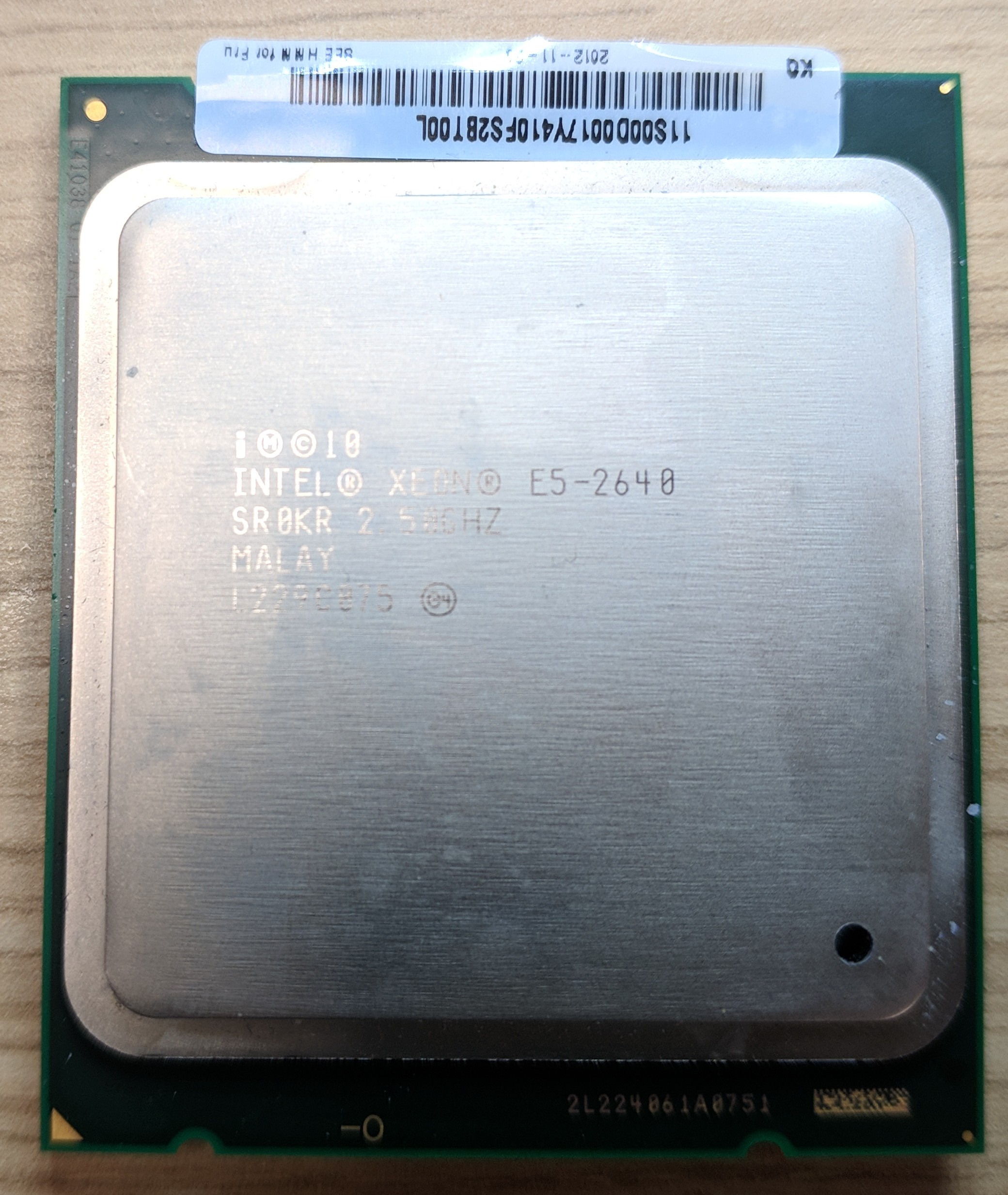 
|
Intel Xeon E5 2640 SR0KR - 2012 This one was part of a pair which both had capacitors knocked off the back. On this one we can see a failed repair attempt. The LGA-2011 socket took Sandy Bridge EP and some Ivy Bridge chips. Some more lowly Sandy Bridges were put on LGA-2011 also. The Sandy Bridge E series supported quad-channel memory, for over 40 GB/s of bandwidth. With their very large L3 caches, they made excellent performers, particularly on large data sets such as SQL Server. Compared to the E5-2603, the three-slice, six core E5-2640 had 15 MB L3 available to it, ran at a significantly faster 2.5 GHz, enabled HyperThreading, and could turbo at 3/3/4/4/5/5. This notation is how much more the multiplier will rise, from the standard (which is 25x on this 2.5 GHz processor from a 100 MHz base clock (BCLK). So, at maximum turbo, it will go to 28/28/29/29/30/30. 3.0 GHz isn't fantastic for Sandy Bridge, but it's certainly not poor. The CPU die was 435 mm², explaining why, even though it ran at 95 watts, these Xeons tended to run cool. With just a mildly ducted 80 mm four-heatpipe cooler of no particular impressiveness, they would hit 65-70 celsius in an all-core workload. A huge die is very easy to get power out of! Intel was reluctant to clock the Sandy Bridge Xeons very high, the E5-1620 was 3.6 GHz (3.8 GHz turbo), but only uniprocessor and the highest clocked of the generation. Six cores, twelve threads, and DDR3-1333 support meant the E5-2640 was eminently competent. It should have been, given that it was over $880 RRP! These guys (yes, two of them) were still in daily use in a Dell Precision T5600 in 2024, with a GeForce GTX 680, two SATA SSDs, and 32 GB DDR3-1333 ECC memory (in 4+2+2 triple-channel per CPU, because that's all I had). They'll likely be replaced by a spare Xeon E5-2640v3 and some "X99" Chinese motherboard within the next year.
|
||||||||||||||||||||||||||||||||||||||||||||||||||||||||||||||||||||||||||||||||
|
CPU Caching
To this point we've discussed the "whats" of CPU caches, but not the "whys" or "hows". So let's compare three CPUs, all with modern three level caches, and their cache design. We'll use AMD's Zambezi, Intel's Sandy Bridge, and Intel's Sandy Bridge-E. All three use their caches as a CPU you can buy today would, and we'll look at some of those later too. In a cache, size and latency are the most important. Associativity is also very important, but in context it is to reduce latency. Latency is, from asking, how long it takes for data from the cache to become available for use, "load to use latency". Latency is measured in clock cycles to avoid different clocks influencing results. In the table below, we are dealing with L1 data cache exclusively. When measuring latency, the results are cumulative, so if our L1 cache takes 3 cycles, and our L2 takes 8 cycles, we will measure 11 cycles for L2 latency since a L1 miss has to happen before an L2 request is made. Similarly, whatever latency our L3 has will have 11 cycles added to it, since we have to check L1 and L2 first.
We're seeing part of what made Bulldozer awful here, the L3 latency was abysmal. While the L2 cache may look bad, 20 cycles for a capacity eight times as large as Sandy Bridge was actually excellent, and Bulldozer's L2 was a high point of the design. What we've seen here is that larger caches, which have to be more highly associative, have to be slower. If we have a 64-way associative cache, then data with a given memory address can be in one of 64 cache lines. A 4-way associative cache has only four cache lines it could possibly be in. To avoid cache lines becoming utterly enormous (and very expensive, as well as getting slow), we increase associativity as we increase cache size. 8-way associativity is considered good, 4-way better. Large caches usually use 10, 12, 14, 16, 18, 20, or even more. The penalty from the high set-associativity is worth the increased cache size. None of this changes with older or newer CPUs! The mere act of being older or newer doesn't influence if a cache is lower latency or more associative. The quick among you will notice that Bulldozer and Sandy Bridge-E were solving the same problem in two different ways and, even today, we still see this balance being used differently by different CPUs. Bulldozer had a large, slow, L2 cache, to avoid L3 cache being much of a problem. If we need to use L3, it's there, but it's not really going to help us all that much - Chances are extremely good the data we need is in L2. Disabling L3 cache on Bulldozer doesn't really hurt you that much, it hurts, sure, but it's not crippling. Sandy Bridge uses L3 very differently. Those little 256 kB L2 caches are optimised purely for speed, that 12 cycle latency is why they exist. This makes L3 cache much more important for Sandy Bridge. It isn't that Sandy Bridge's L3 cache is good because it's fast, it's fast because it has to be. Disabling L3 cache on Sandy Bridge is catastrophic, which is why Intel used L3 as a segmentation feature. For many years, a desktop i5 would have 6 MB L3 cache and the i7 made from the same silicon would have 8 MB. Let's do this comparison again, but use Intel's Raptor Lake and Alder Lake (P-cores only), AMD's Vermeer, and AMD's Vermeer-X. We'll include Matisse too. Matisse did technically have 32 MB, but it was split in two 16 MB blocks, one for each core complex (CCX) of four cores. As a victim cache, there was little inter-CCX communication needed.
Now we see the same two approaches to caching again, a decade later. Raptor Lake is betting the farm on that 2 MB L2 cache and its L3 cache is more of an afterthought. In Alder Lake, L3 runs at a reduced "uncore" speed, which is variably clocked, and L3 latency can get very, very high if E-cores are accessing it, since the uncore doesn't throttle up if the only load is from the E-core clusters. Raptor Lake's uncore does clock up when E-cores are accessing L3, which is an improvement, but here we are only measuring P-cores. Without sharpening the spear overly, Intel's L3 cache is awful for performance. Just like Bulldozer, however, it can be, there's that 2 MB of L2 cache at 16 cycles insulating the cores from L3. L3 here is a power-saving measure, not a performance boosting thing. L3 cache runs on the uncore clock, usually around 3 GHz, and Intel normalised ring latency in either Haswell or Skylake, so the most distant ring stop is the same latency as the nearest. Hitting L3 cache is much lower power than going out to DRAM even if, in Alder Lake and Raptor Lake, the latency is actually similar. So what Intel's doing here is saving energy, which makes absolutely perfect sense: Intel's core market is laptop CPUs. Moving from L2 cache, which is on-core, to L3 cache on-die is expensive in energy. Moving from L3 cache off-die to DRAM is even more expensive. AMD has come full circle. Zen 2 and Zen 3 have identical L1 and L2 caches, L1 is pretty standard these days, L2 is moderately large, but aims to be low latency... And succeeds at it. AMD's glory here isn't the fast L2, though, it's whatever the hell it's managed to do with L3. AMD doubled L3 from Matisse to Vermeer (Matisse had 2x 16 MB, with massive latency between them) and increased latency by only 12 clocks. In Vermeer-X, L3 is tripled for an extra three clocks! AMD has a very different approach to Intel here. Where Intel sees L3 as a power-saving device to avoid DRAM and is betting performance on the big L2, AMD sees L3 as a performance booster. Sure AMD could get away with a 50-60 clock L3 latency, of course it could, but AMD's in the performance game here and, in Vermeer-X's case, in the game performance. Many often ask "Why doesn't Intel just give its CPUs a massive L3 cache and catch up with AMD's X3Ds?" and here we have the answer. Intel already has most of the benefit from its huge L2 caches and Intel's L3 isn't intended to raise performance, it's intended to save power. | |||||||||||||||||||||||||||||||||||||||||||||||||||||||||||||||||||||||||||||||||
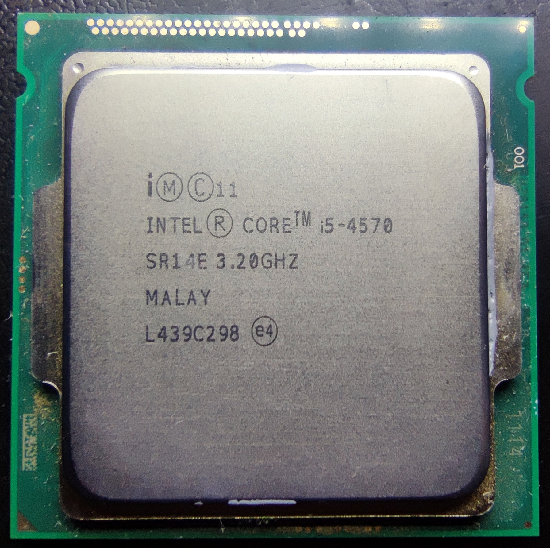 |
Intel Core i5-4570 SR14E - 2013 About $230 in mid-2013 got you the mainstream Core i5 of the Haswell generation. It ran a base of 3.2, a boost of 3.6, a TDP of 84 watts which it would normally not get anywhere near, and ran a GT2 IGP (80 EUs in most SKUs) at 1.15 GHz from the Haswell 4+2 silicon. Intel's desktop mainstream of late 2013 mostly continued the patterns of Ivy Bridge. Compared to the i5-3570 it replaced, the 4570 dropped all clocks by 200 MHz (dropped?!), retained DDR3-1600 support, same 22nm manufacturing, 2 MB of the 8 MB L2 cache is turned off (6 MB total) kept more or less the same iGPU, and changed the socket for no reason other than to generate e-waste. (And to support the quickly abandoned FIVR) The new 8-series chipset, mandatory for Haswell, boosted up USB a little and enhanced xHCI support, but that's about it. This was minimum effort, minimum product. On release, the mainstream reviewers all toed Intel's line, and never included a direct comparison with its predecessor. This is always a red flag. Typically i5-4570 was 95% of the performance of the i5-3570. Haswell's architectural improvements could not make up for a 200 MHz clock deficit. Intel specifically misled and placed its launch-day review samples to avoid comparisons. The review samples given to major sites like AnandTech were the i7-4770K and i5-4670K, while the non-K i5-4670 was the like-for-like replacement of i5-3570, not just in specification, but also in price. Yes, dear reader, Haswell was not a generational improvement. It raised price around 10%, raised power around 10% and, in some cases, raised performance by 10%. Was mighty Intel beginning to falter? Were there fundamental problems with the basic Nehalem architecture, of which Haswell was another improvement upon? Well, the answer to those was "No". Intel had no reason to push ahead as it had no competition. AMD was at its lowest ever ebb and, while not completely uncompetitive, it was not able to fight in the top levels of performance. Without the push from AMD, Intel chose to progress slowly and carefully. Large generational leaps were risky and expensive, so Intel shied away from them. Haswell was not changed microarchitecturally much from the Sandy Bridge architecture (which Ivy Bridge also used unchanged) and was instead meant to adapt the design to non-planar "FinFET" transistors and also bring power usage down. Total package power went up, as the power-hungry voltage regulators were brought on-die as "fully integrated voltage regulator" or FIVR, but this brought total system power down. These components used less power on the die than on the motherboard but could also switch faster, meaning Haswell could get to peak turbo clocks on a core from sleep in 420 nanoseconds (320 to wake, 100 to clock up). Intel's 2012 ambition of moving more to near-threshold voltages was also supported by FIVR. A few years later, Skylake did away with the FIVR and it hasn't been seen since. Did Haswell at least fix the awful thermal interface material under the IHS which had annoyed us with Ivy Bridge? No. No it did not. While rated at 84 watts TDP, the Haswell i5-4570 had a 1C/2C/3C/4C turbo table of 36,36,35,34. In use, even with heavy load on the IGP, this was unlikely to cause more than around 45-60 watts total package power. This particular sample came out of a Lenovo ThinkCenter M83 SFF, which definitely didn't have a heatsink rated for 84 watts in it.
|
||||||||||||||||||||||||||||||||||||||||||||||||||||||||||||||||||||||||||||||||
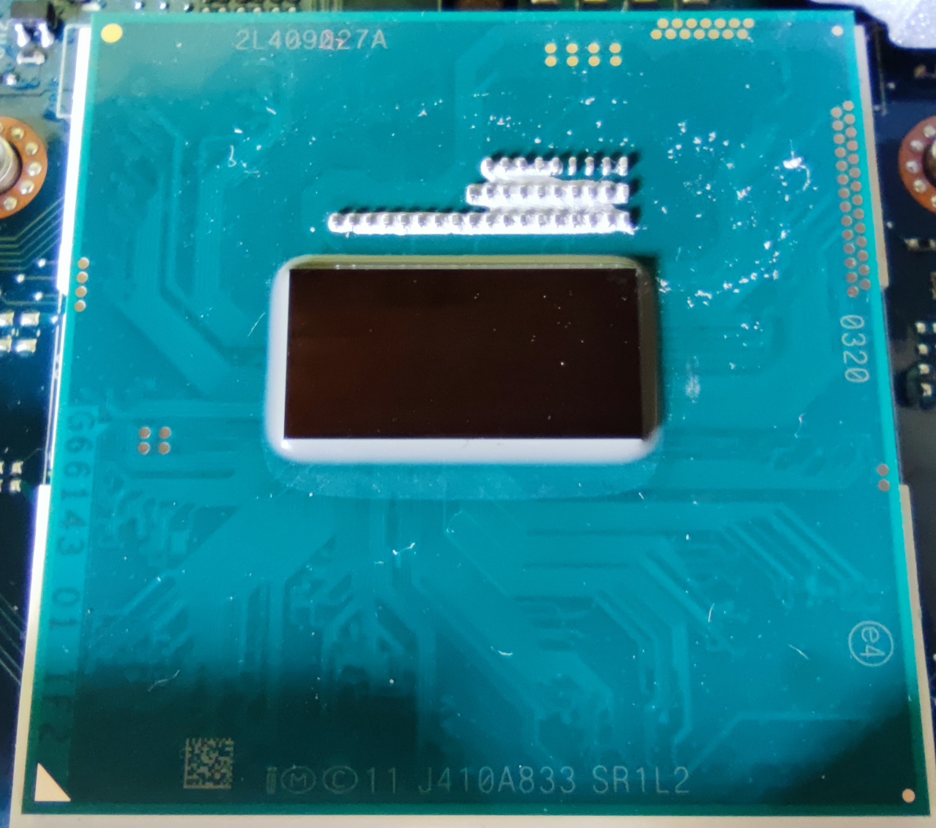 |
Intel Core i5-4310M SR1L2 - 2014 This Haswell based mobile processor was based on the very lowest tier of Haswell silicon, and was provided as dual core, 3 MB L3 cache, as part of the early 2014 Haswell Refresh. Intel generally bumped clocks a little at the same power and price as Haswell on 22 nm yield improved and economics allowed. Graphics Tier 2 was enabled here (as Intel HD 4600) with 20 execution units. Intel got a lot of mileage out of this silicon, it did all the mobile Celerons, Pentiums, i3s and i5s. The dual core i7s (ultra-lights) were made from this same silicon, but had all 4 MB L3 cache enabled. Intel's last level cache here was 2 MB per core, but here we had only 1.5 MB per core enabled.  Source: WikiChip (this is actually Haswell 2+3, not the 2+2 in use here) Spot the features: 1 MB L3 cache segments in green, memory controllers just below them (smal blue boxes), L2 cache as pale blue boxes in the cores (top), then the cors themselves between the red lines on the right, above the green L3 blocks. Finally, on the left, sixteen pairs of GPU execution units. Haswell was wider and more power hungry than Ivy Bridge, but delivered around 10% more clock for clock performance. The GPU, slightly updated for DirectX 11.1, was otherwise very similar to that in Ivy Bridge and would clock as high as 1250 MHz in this i5-4310M. For a laptop which wasn't CPU support whitelisted, such as the Dell Latitude E6440 this lived in, the fastest CPU is the Core i7-4610M (4C/8T,4 MB L3) due to the 37 watt TDP being the limit. 47 and 57 watt parts were also available, but the E6440 had nowhere near enough heatsink for those. As new, from Dell, the E6440 was configurable with the i5-4200M, 4300M, 4310M, i7-4600M and 4610M, as well as a number of i3s which aren't worth mentioning. It's possible the 37 watt i7-4712MQ would work, from the Haswell Refresh, but that'd be based on BIOS support. Confusingly, Intel brought back the Pentium G3420, a part based on this same silicon, first launched in 2013, in 2019! It was still available even as it reached end of life in June 2021.
|
||||||||||||||||||||||||||||||||||||||||||||||||||||||||||||||||||||||||||||||||
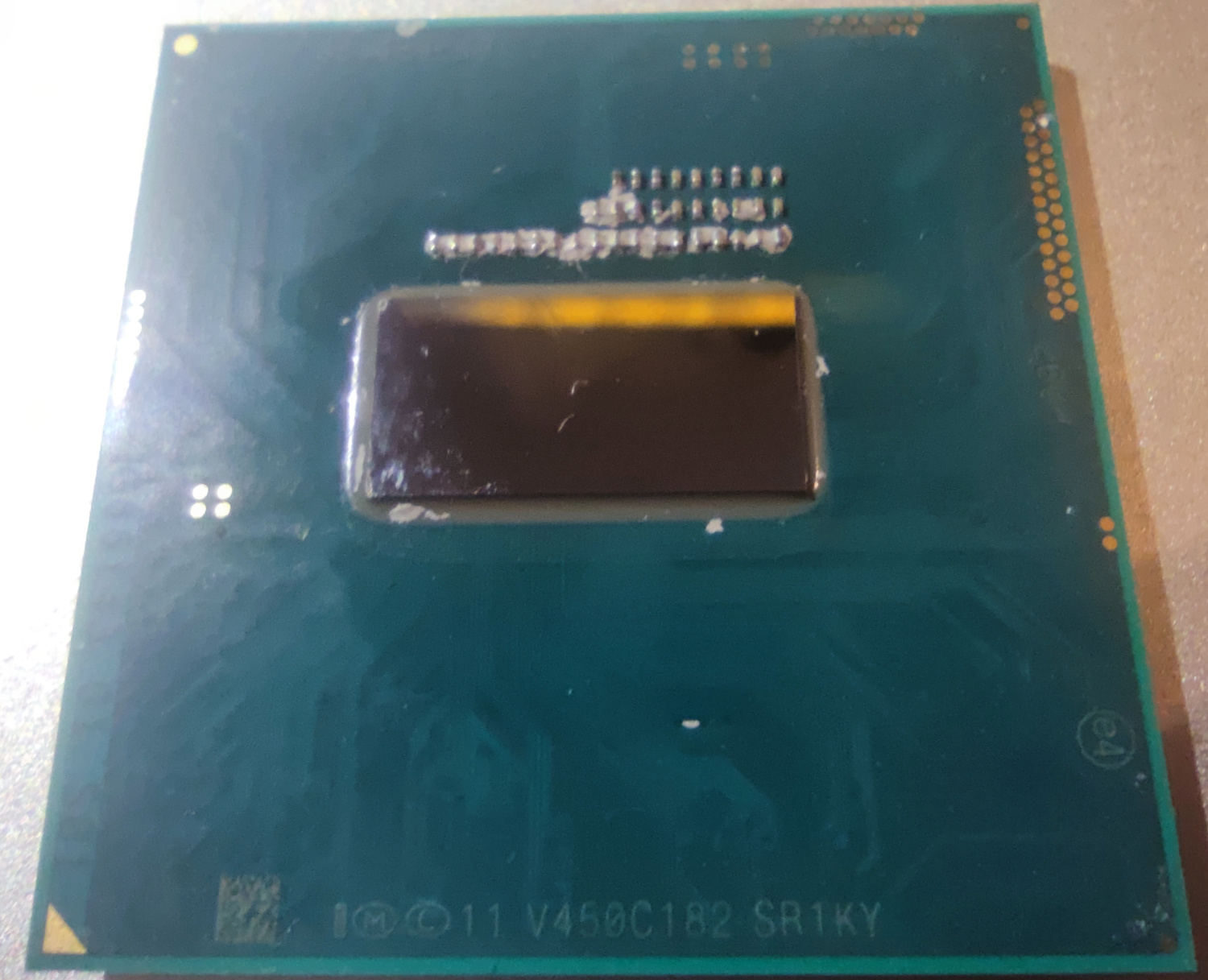 |
Intel Core i7-4610M SR1KY - 2014 The Haswell mobile i7s were often dual core and this was one of the most common. Part of the Haswell Refresh, it sported two cores with a maximum clock of 3.7 GHz, 4 MB L2 cache, and a TDP of 37 watts. The IGP runs at a maximum of 1.3 GHz. The model numbering system we liked so much in the Penryn and Wolfdale days had become a complete wreck by this point. It came out of a laptop which was seemingly smashed up by some kids next to a road and seems to have taken a chip to the die, but it was fully working. Also in the same laptop was a Crucial MX100 512 GB SSD (fully working) and 4 GB Samsung PC3L-12800 RAM (untested), a DDR3L-1600. The laptop was identified as either a Dell Latitude E6540 or its Precision M2800 equivalent. It had a discrete GPU fitted, so was likely the Precision M2800. It would have been a formidable machine in its day, and still quite capable in 2022. 4 GB was on the low side, and it was in single channel (though this doesn't mean to say a second SODIMM wasn't ever present) which would reduce performance of an otherwise high end laptop. The i7-4610M is worth comparing with the i5-4310M just above. They're the exact same silicon! It's natively dual core (the quad cores were "QM"), has a the same 20 EU GPU, and each core "slice" has 2 MB L3 cache, with 0.5 MB of that disabled on the i5. The i7 has all L3 cache enabled and all GPU enabled. So what did the i7 monicker get you? Basically, one megabyte of L3 cache. With the i7-4610M being fairly boring, we'll have a talk about the GPU architecture. The sharp eyed in the audience, reading the i5-4310M entry, would could GPU segments (EUs) and reach the conclusion that there's 32 of them, synthesised in blocks of four. Each EU has 8 ALUs so these GT2 with 20 EUs enabled had 160 ALUs. Did Intel really disable 12 EUs per die, on every GT2 product it made? Was any Haswell GT2 fully enabled? What was going on? The Haswell family had six major parts. Let's list them: Haswell 4+3: Four cores, 1.5 MB L3$ each, GT3 GPU, all with eDRAM Haswell 4+2: Four cores, 2 MB L3$ each, GT2 GPU Haswell 4+1: Four cores, 1.5 MB L3$ each, GT1 GPU Haswell 2+3: Two cores, 2 MB L3$ each, GT3 GPU Haswell 2+2: Two cores, 2 MB L3$ each, GT2 GPU Haswell 2+1: Two cores, GT1 GPU 2+3 and 2+2 also had ULT variants which trimmed L3 cache down by 0.5 MB per core The attentive have got the solution already: Did we inadvertently used a die shot of Haswell 2+3, not the 2+2 which was actually used? It appears we did (and have corrected the record above)! Intel's PR machine published beautiful colour coded die floorplans of 4+2 and 2+3, but not the vastly more common 2+2! So, we're gonna have to fake one. The actual 2+2 die is something like this image:  A somewhat crude faked image of what Haswell 2+2 would look like There! 20 EUs exactly as Intel specified! The fakery was done by using the 4+2 image as a guide to replicate and trim parts of the 2+3 die. So anyway, what did the i7 get us over the i5? CPU clock: The 4610 ran at 3 GHz and turboed to 3.7 GHz. The 4310 ran at 2.7 GHz and turboed to 3.4 GHz. GPU clock: 20 EUs at 1.3 GHz vs 20 EUs 1.25 GHz. Pretty much nothing. L3 cache: 4 MB vs 3 MB. Price: $346 vs $225 And that's it! You paid $121 more for essentially a minor speed grade uplift. It was almost unnoticeable. As for this guy? There's a minor chip off the corner of the die but it didn't cause any issues, and the CPU is now in a Dell Latitude E6440 with 16 GB RAM and an SSD. The 37W TDP is a little more than the Latitude can handle, it tends to be able to sustain 28-30 watts power, but it's certainly not as egregious as something like the i7-4712QM, also rated to 37 watts. This was Intel's last socketed laptop generation before it became BGA exclusively, the "ultrabook" form factor, which sacrificed everything on the altar of thinness. Most laptops today use this thinner design (typically with an aluminium unibody) but it caused thermal constraints. The equivalent of this CPU later (2023 timeframe) is probably the i7-1355U which can boost up to 55 watts, but typically is rated for 15 watts. It has ten cores, but only two of those are full performance cores, the remaining eight are slimline, slower, "efficiency cores". Clock for clock, those "e-cores" are actually quite comparable to the ten year old Haswell cores here! Coincidentally, they also run at 3.7 GHz maximum.
|
||||||||||||||||||||||||||||||||||||||||||||||||||||||||||||||||||||||||||||||||
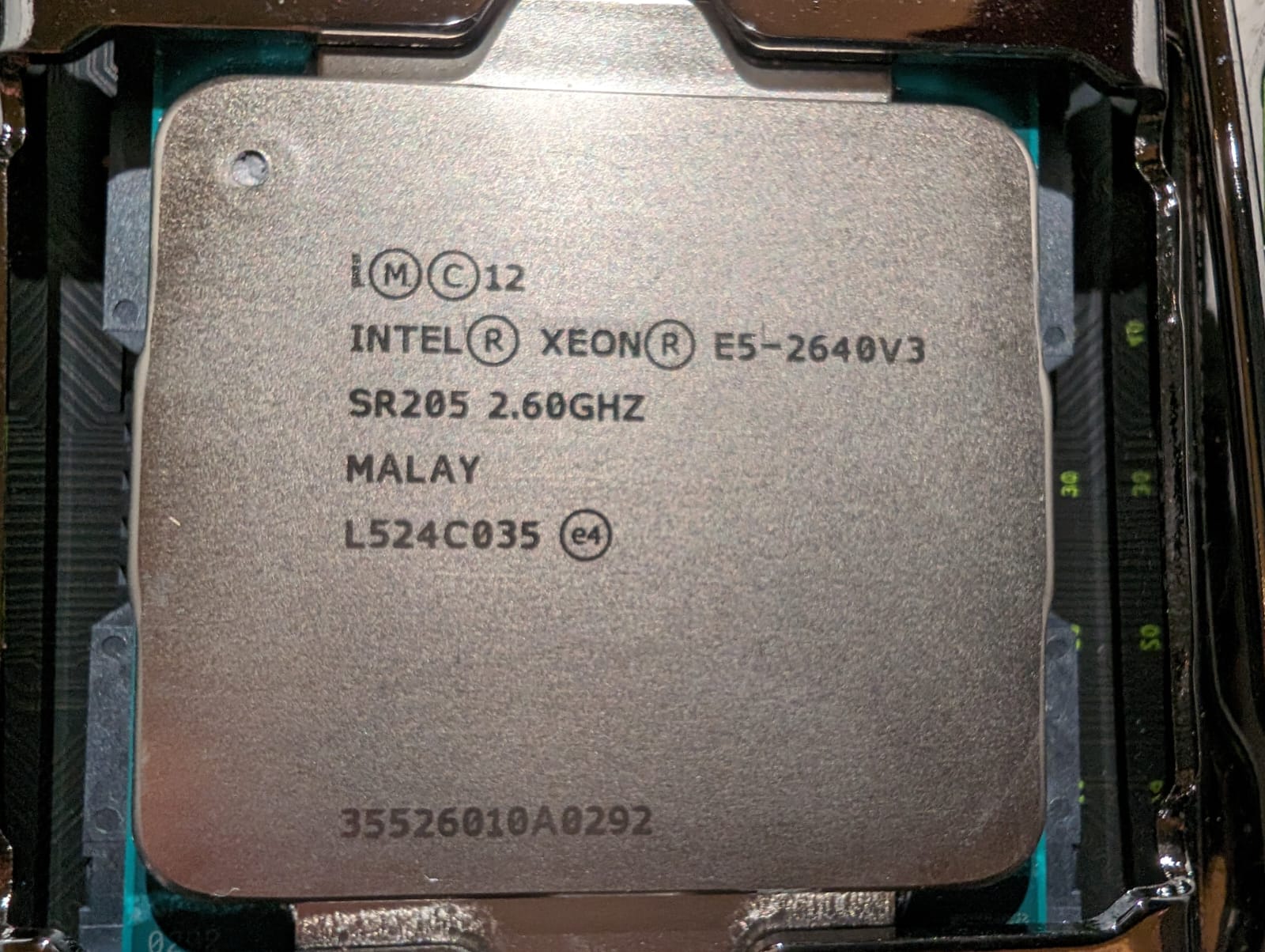 |
Intel Xeon E5-2640v3 SR205 - 2014 While Intel's consumer ("client computing") line was being refreshed with Haswell Refresh in 2014, the Xeon line was also being updated from Ivy Bridge to Haswell. In Q3 2014, the Xeons dropped, using two distinct silicon dies. You'll see Haswell-EX and Haswell-EP being quoted, but these are marketing lines, not dies. EX was "High End Desktop" or HEDT, while EP was server. Haswell 4+3 (Quad core GT3) was the largest client die at 260mm^2, not widely used, very expensive, and used an eDRAM L4$ for its very capable IGP. (This eDRAM, Crystalwell, was not density optimised as most DRAM, but instead latency optimised, it was extremely impressive!) Client CPUs have to spend a lot of die area in the IGP part of the die, around half of it, but servers have no need for that. What servers needed were more cores and more connectivity. So, the top end client had 28 PCIe lanes and four cores. The E5-2640v3 here has 40 PCIe lanes and eight cores! It occupied a much larger die, at 355mm^2, and had no IGP at all. The other major change was L3 cache on the Big Boy Haswells. All clients had 1.5 or 2 MB L3 cache per core, but the server CPU here sported 2.5 MB per core, for a maximum of 20 MB. There was another Big Boy Haswell, and he really, really, was big. At a frankly grotesque 622mm^2, it was running for the largest single silicon die ever commercialised. It had eighteen cores but also had two rings. Intel's ring bus is the CPU's internal way of connecting its "ring stops", and each ring stop is access to L3 cache of each individial core. Each core can access every L3 cache of every other core at the same speed as its own L3 cache, and the ring runs at the "uncore" clock, commonly 3.0 GHz in this era. On the 18 core variant, the two rings had to go out a step further to talk to each other, so CPUs on the 10 core ring had a higher latency when requiring data from the L3 cache on the 8 core ring, so we called this architecture "10+8". The E5-2640v3 here was not from a 18 core die, but from an 8 core die. It arrived here almost for free in early 2024 as part of an "X99 Bundle" on Ali Express. With 16 GB RAM and a B85 (C220) motherboard, it was a shockingly cheap offering at just £87 for everything. The motherboards were built around either recovered or "new-old stock" chipsets, and the Xeons were all recycled e-waste, but they were all tested before sale. This system replaced the previous Core i5-3570K in the box running hattix.co.uk and home server duties in early 2024. It was replaced by a Xeon E5-2490v4 a few months later which was almost worryingly cheap, £33 shipped, and 14 cores!
|
||||||||||||||||||||||||||||||||||||||||||||||||||||||||||||||||||||||||||||||||
|
Thermal Design Power (TDP) We talk a lot of TDP, but what exactly is it? Initially, it was quite easy. It was the maximum power the CPU was ever going to use. The TDP of an AMD Athlon 1.4 GHz with the "Thunderbird" core was 72 watts and that was as high as Thunderbird ever went. So, if your heatsink or however you dealt with thermal power could handle 72 watts, while keeping the CPU from reaching its maximum operating temperature, you were golden. 72 watts was quite a bit of heat back then so you needed something substantial to cool it. While a reused Socket 7 cooler would fit, it would not be sufficient (and was a bad idea for other reasons too). When Intel's SpeedStep moved from mobile Pentium-IIIs to desktop Pentium4 CPUs, in around 2003, TDP changed its meaning. These CPUs could thermally throttle: If they hit a maximum temperature, they ran a duty-cycle to reduce their power consumption. Most higher end Pentium4s would exceed 100 watts electrically while only sporting a 70-80 watt TDP, so they would throttle even if your cooler met Intel's spec. In most workloads, however, they would not throttle and so Intel's spec was sound. This more or less brings us to the era of 2012-2018. When running cool, CPUs were able to clock much higher than they otherwise would, so "boost clock" or "turbo clock" became a thing. As their higher clocks caused higher power consumption and temperature rose, they backed down to balance the two. Laptops had been doing this for years and CPU designers started using it on desktops too, to allow even higher power usage and higher performance. Of course, Intel had to formalise it. Becuase Intel. "Turbo Boost Technology" obeyed a number of duration and level limits, because of course it did, so even when running cool, an Intel CPU would reduce its performance for no physical reason, only that it had been running fast for a set duration of time. Intel's Turbo Boost 2.0 defined "Power Level 1", "Power Level 2" (PL1, PL2) and "Tau". Power level 1 was the basic "I can do this forever" power while under load. PL2 was a special much higher power level intended for use only in short durations. "Tau" was the duration of time PL2 was allowed to run for. All this was under motherboard and system firmware control, as they knew how much power the system VRMs were capable of and could order the CPU to back down if the VRMs were getting too hot. So, on a Core i7-10700K, PL1 was set at 95 watts, PL2 set at 175 watts, and Tau defaulted to around two seconds. Most desktop motherboards set Tau to a huge number to allow more CPU performance so the CPU was always able to do PL2. AMD was doing something similar with its Precision Boost system (derived from the Skin-Aware Thermal Power Management of AMD's earlier laptop CPUs). This monitored some very badly named parameters, electrical design current (EDC), thermal design current (TDC), and package power tracking (PPT). The EDC was the maximum power the motherboard's VRMs were able to provide. On a desktop motherboard this could be extremely high, topping 300 amps. TDC was the power the VRMs could provide indefinitely, without causing them to overheat. Again, this could be extremely high, usually north of 200 amps. With, say, a Gigabyte B550 Aorus Elite AX V2, these were set to 460 amps and 320 amps, which told the CPU it could peak at 460 amps, but only sustain 320 amps. For most AMD AM4 CPUs, these limits were far beyond what the CPU would ever be using. The motherboard makers used this as a bit of a crutch. An AM4 CPU was practically never going to sustain north of 200 watts (a 5900X or 5950X could do it, if heavily overclocked) which would require >300 amps from the VRM, and the motherboard's VRM units were rarely actually able to run that high. The CPU would then boost its clocks up to its maximum boost clock (although Precision Boost Overdrive, PBO, allowed this to be exceeded by up to 200 MHz in most cases) while remaining within the EDC, TDC, and the package power tracking (PPT) fed back to the algorithm based on temperature. At the maximum allowed temperature, typically 90-95 celsius, PPT would start to be reduced to keep the CPU from exceeding maximum. PPT was also a limit, and would feed back if the CPU hit the PPT limit. With Precision Boost Overdrive, these limits could be changed, usually raised, to unlock additional performance. "Eco Mode" was basically PBO with a lowered PPT limit, so a 65 watt CPU (PPT of 85 watts) would be reduced to 45 watts. This limited maximum performance, usually by around 5-10%, but made the CPU run way more efficiently. For example, a 65 watt AM4 processor (e.g. Ryzen 5 5600X or 5700X) would have a 60A TDC requirement, a 90A EDC requirement, and usually an 85 watt PPT limit. In "Eco Mode" this was down to 45 watts. Under PBO with all limits relaxed and a good cooler, the maximum observed power is about 105 watts. This is now us completely up to speed. Power and temperature are now seen as resources to be used if possible. If we're rated for 90C and only running at 80C, that's 10C of thermal headroom we're not using, so we can boost power some more, use that headroom, and run faster. This often causes panicked neophytes to post questions about their "overheating" CPU, when they don't actually understand it is neither overheating, nor in any danger. It also induces them to buy far larger coolers than they actually need, which I'm sure the AIO manufacturers don't mind at all. Yes, there are people out there with triple fan 360 mm AIOs on 65 watt CPUs. If they could see how small a heatsink they actually need, they'd probably react with disbelief! |
|||||||||||||||||||||||||||||||||||||||||||||||||||||||||||||||||||||||||||||||||
 |
AMD Athlon X4 880K - 2016 Go home AMD, you're drunk. The Godaveri or Kaveri Refresh CPU design used the Steamroller CPU core, a refinement of Piledriver (which set nothing on fire but itself) which was in turn a refinement of the original Bulldozer release. Steamroller had been previously used in Kaveri from the previous year. The new Excavator cores were available and shipping, but AMD felt it was cheaper to just rework the already-designed Kaveri designs. It was unclear what Kaveri Refresh actually refreshed. The manufacturing process had been moved from silicon-on-insulator (SoI) to just cheap bulk silicon, as GlobalFoundries couldn't do SoI at 28 nm, so the process for Kaveri and Kaveri Refresh was plain GlobalFoundries 28SHP. Kaveri and its refresh were both 245 mm^2 dies, both with two Steamroller modules, both with second generation GCN GPU architecture (8 compute units), both with DDR3-2133 support... Very little changed. Kaveri was old hat when this 880K was released in March 2016, having first been released in mid-2014. The 880K boosted clocks a little, a base of 4.0 GHz and a turbo of 4.2 GHz, in a 95 watt TDP. The GPU in the Athlon X4 was disabled, which was frankly bizarre for the FM2+ platform, designed for APUs with onboard video, especially with AM3+ sitting around. This came out of one of the worst pre-builts I've ever seen. Ever. It came here because it was running slow, so what was wrong? Well... The quick among you have seen the problem already. Those are copper marks on the CPU heatspreader. There was no thermal interface applied. At all. To a 95 watt CPU. The PC it was in, sold as a gaming machine, was £700. £700! It was sold though one of those predatory "buy now pay later" companies, when it was in fact a basic £300-£400 machine. Basic Seagate HDD (not even an SSD!), basic GeForce GTX 1050Ti 4GB, basic single stick of DDR3, basic tiny Gigabyte GA-F2A78M-HD2 motherboard (only five power phases, none of them with heatsinks!), far too many fans, far too large a case, and far too high a price. It arrived here in 2023 as it was too slow for even light gaming and daily OS tasks. With instructions to not spend much on it, I instead replaced the RAM with two four GB sticks (getting dual channel), then fixed the CPU overheating. There wasn't much else possible on the FM2+ platform, the 880K was already the fastest CPU possible on it. Worse still, the PSU had a single PCIe 6-pin so it'd also need to be replaced for anything serious. Anyhow, back to the CPU. All else equal, the Core i3-6300 wiped the floor with it in games. It'd overclock as far as around 4.5-4.6 usually, gaining around 10%, but remaining well behind the i3-6300. However, the 880K was dirt cheap, available for less than £75 in most places. That's why I disparaged the "gaming" PC so much. For £700, it had a £75 CPU, a £80 motherboard, £40 of RAM, a £35 HDD, a £80 case, and a £150 video card. I add that up to £460 and those are retail prices. The recommendation for a budget games machine is always "cheapest CPU possible, and throw it all at the GPU", which is exactly what's been done. Only, you know, build it properly.
|
||||||||||||||||||||||||||||||||||||||||||||||||||||||||||||||||||||||||||||||||
 |
Intel Celeron N3060 SR2KY - 2016 Let's say you want the cheapest, tiniest, most basic x86 SoC (system on chip) which could still be a legitimate SoC. You wouldn't end up far from the Celeron N3060. It used Intel's Braswell SoC, which replaced Bay Trail at the very bottom of everything. The Atom branding was still being used at this point, and the Atom x5-E8000 was implemented by Braswell. As the Celeron N3060, it ran at 1.6 GHz with a potential boost up to 2.48 GHz in a TDP envelope of just six watts. The Airmont cores, of which two are present, are joined by 12 Gen8 execution units for graphics, which run at a base of 350 MHz and boost up to 600 MHz. Braswell had two 32 bit memory controllers, usually running to a single 64 bit SODIMM in laptops, but a single 32 bit mode was also available, if bandwidth from 20 years previous was desirable. Of course, it was intended for the extremely low end of things. The silicon itself had 4 Airmont cores, 18 graphics execution units (arranged in three "subslices" of 6 EUs), and 2 MB L2 cache. All of these were only ever enabled in the Pentium J3710, which was a bizarre 6.5 watt desktop processor, overlapping AMD's equally bargain basement E-series of Bobcat and Jaguar based SoCs. On mobile, the Pentium N3710 was more or less the same thing. How much of the Braswell silicon was enabled here? The answer is "a bit over half." The full SoC had four Airmont cores, 2 MB L2 cache (shared), 18 GPU execution units , eDisplayPort, HDMI, DisplayPort, PCIe x4, USB3, USB2, and SDIO. The Celeron N3060 disabled half the Airmont cluster and a third of the GPU. The three SATA2.0 ports were disabled, only exposing the two SATA3.0. Even at this bargain basement level, Intel couldn't resist the castration of its products. How bad was it? Well, Intel had a pre-planned product refresh in mind with Braswell (and Haswell), where the Q1 2015 releases would be replaced by Q1 2016 releases of the same silicon with some clock bumps. This enabled Intel to keep prices up on aged silicon! The N3060 (2016) and N3050 (2015) differed only in their single core maximum turbo, which was 2.48 and 2.16 GHz respectively. The N3010 and N3000 also differed only in the same way, 2.24 and 2.08. Intel claimed "Turbo Boost Technology" was not available on Braswell, but they still scaled their frequency above base all the same. This is a hard demonstration of what a monopoly looks like. AMD wasn't very competitive at this time, so Intel could abuse the hell out of the market. AMD was, however, competitive at the very low power end, with the new Jaguar-based SoCs. The Atom x5-E8000 was one of the most powerful members of the Braswell family and was less than one quarter the price of the Pentium J3710, the most powerful, and was still under 40% of the price of the Celerons. Why? The embedded market Intel was aiming Atom at was much more competitive and AMD was practically owning it.
|
||||||||||||||||||||||||||||||||||||||||||||||||||||||||||||||||||||||||||||||||
|
Why no 5th generation? or Broadwell, What Went Wrong? At the end of 2014, Intel was seemingly unassailable. AMD was stuck on its Bulldozer architecture, which did everything right except the L1 cache, resulting in it doing nothing right. Intel's 22 nm had high yields and had just refreshed Haswell with process gains to enable slightly bumped clocks at the same power and 14 nm was around the corner. Everyone else was on 32 or 28 nm. A few years before, the Sandy Bridge architecture had leapt ahead by a massive amount. This was the way of the world and how things were. Of course Intel had a process advantage, it always did have. Intel was first to commercialise a new process all the way back to the 1990s. First to 350 nm, 250 nm, 180 nm, 130 nm, 90 nm, 65 nm, 45 nm, 32 nm, 22 nm... Of course Intel would be first to 14 nm. Then Intel would port Haswell to 14 nm as Broadwell, release the 5th Core generation, just as the world should be. Cracks started showing. Intel Developer Forum was used as a vehicle to show how Intel's process leadership was still on track, by showing 14 nm yields against 22 nm yields, but only labelled the axis of the 22 nm yields. Haswell Refresh was touted as a great thing, a fine demonstration of Intel's 22 nm leadership, when it only existed to buy time. The easiest manufacturing for any process to do is mobile and low power. These chips won't clock high, won't need higher voltages, so are a lot easier for a struggling manufacturing process to produce. Intel used the low power silicon to produce the Xeon E3 and Core i5/i7 embedded "-R" processors, all intended for embedded application. This silicon had four cores and 24 GPU EUs with the eDRAM controller for Crystalwell. It was also used for the Core i7 "HQ" mobile processors. Even though it was low power manufactured, it was also used for the only two desktop processors released, the i7-5775C and i5-5675C, which both sported 128 MB Crystalwell eDRAM. Another low power silicon variant existed which didn't have the eDRAM controller and only had two cores, but retained the 24 GPU EUs. This was the non-HQ Core i7 mobile and all of the Core i5 and i3, as well as the much lower-end Core M. The high power silicon was used only to make Xeons, the Xeon E5 v4 series. Skylake was nearing completion and would sell better if Intel hadn't just released Broadwell on desktop. After 14 nm finally got shipping, it was so full of workarounds and fixes that it was both very expensive and the lowest yielding CMOS process Intel had ever commercialised. Now Intel had two problems: 1. It had only just managed to make 14 nm work 2. 10 nm was next and an enormously larger challenge Intel spent the next five years trying to get 10 nm working and, initially, fixing the mess that 14 nm was. By the time of Coffee Lake (8th & 9th gen), 14 nm had yields up around as high as 22 nm had been, but 10 nm was still not remotely ready for commercialisation. A single mobile SKU, which couldn't even get its IGP working, was all the entire Cannon Lake generation had. So for Comet Lake (10th gen) and Rocket Lake (11th gen), Intel had to keep improving 14 nm. Comet Lake was reasonably okay and competitive, but Rocket Lake was a regression in almost every area. It ran slower than Comet Lake, used more power to do so, and it was like AMD's Zen 3 hadn't just been released beating Comet Lake at everything, in everything. Intel had gone from unassailable to unlovable... Yet, Intel had not yet reached its nadir. |
|||||||||||||||||||||||||||||||||||||||||||||||||||||||||||||||||||||||||||||||||
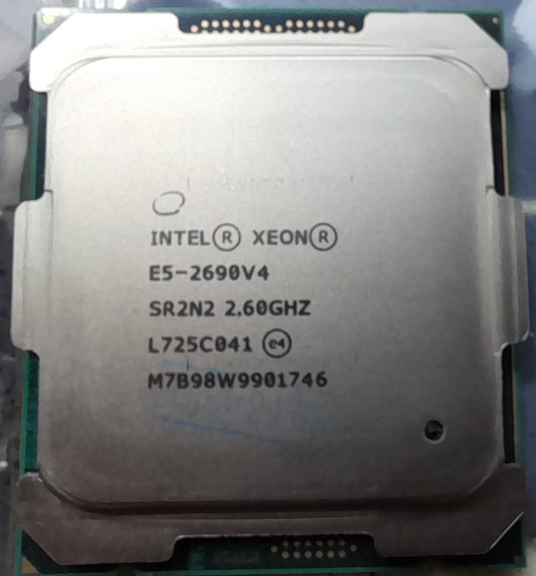 |
Intel Xeon E5 2690V4 - 2016 The v4 Xeon family was Broadwell, a fairly direct 14 nm shrink of Haswell with some minor architectural updates the engineers wanted in Haswell but didn't have time for. We'll do two quick comparisons, one between two similar Broadwell Xeons, and one with the product Intel invited comparisons to, the 2690v3.
This raises almost more questions than it answers. The 2680v4 was just 200 MHz lower across the board and the same price. They launched on the same day in early 2016 (a year and half after the Haswell-based 2690v3) and were 19.7% more expensive. Removing the 2680v4 (which was just there to show the absurdity of Intel's MSRPs, they aren't what anyone pays), all we get are two more cores and slightly faster DDR4 support. Haswell Xeons did 2133 MT/s, while Broadwell bumped that to 2400 MT/s. Were those two more cores worth an extra 19.7%? They were the same speed, after all. That 19.7% more cost, a year and half later, got you 16.7% more cores, which only made any difference at all if you were already using all 12 cores. This is why Broadwell didn't get much of a consumer release. It didn't clock higher, it didn't use much less power, and it was the same Haswell architecture. How had mighty Intel got a "tick" release wrong? The architecture was completely unchanged from Haswell! All they had to do was just do the layout for the new dies. The three dies available were also architected the same as Haswell. A 22 core "High Core Count" die at 454 mm² had two ring buses (11+11), connected by two bridges, and could present as two NUMA domains. A 15 core "Medium Core Count" die (never sold with all 15 enabled) at 306 mm² had a 10+5 ring system, also able to do NUMA, while a 10 core "Low Core Count" die had a single ring bus and covered 246 mm². All these counts were up from Haswell, demonstrating the density of Intel's new 14 nm process, but per-core power was not down that much at all from 22 nm. Per-core L3 cache was 2.5 MB in all Broadwell Xeons. Other dies were consumer focused, but none of them made for high power. A tiny 82 mm² due had two cores and 12 GPU EUs, a slightly larger consumer die had the same two cores and 24 GPU EUs (taking up most of the die!), a quad core with 24 GPU EUs at 182 mm² would presumably have made the mainstream desktop/laptop of that era but saw extremely limited release. Back to the question at hand: Why did Broadwell falter? Why was it only popular among laptops and servers? For servers, the silicon density was the key player. Intel's production cost was much lower than Haswell, so it sold Broadwell as a "drop-in" replacement for Haswell. For mobile, the low-power focused variants were still that bit cheaper to manufacture, but also could hit good performance at lower power than Haswell could, a direct benefit. 14 nm was a year late so, by the time Broadwell was available, Skylake was just around the corner with large increases in performance. For mainstream desktops, though, none of these advantages mattered. Desktop silicon isn't made with low power libraries, so that benefit was gone. It also isn't high margin, so the density benefit was reduced. It wants high clocks... Which Broadwell couldn't deliver. Only two "proper" desktop processors were released, in 2015, the Core i7 5775C and the Core i5 5675C, which both clocked low, and used the low power optimised silicon from the mobile market. There were some relabelled Xeons, sold as Core i7 6800K, 6850K, 6900K and 6950X, which went on the LGA2011-3 socket, used the Low Core Count silicon and, for typical desktop use, underperformed the Core i7 6700K. Part of the reason was Broadwell's architecture. The fully-integrated voltage regulator appeared to have either caused scaling problems, yield problems, both, or other, because Intel abandoned it in Skylake and never revisited it. Intel's 14 nm process was also a year late to production, meaning there were problems with it. Anyway, that's enough of our background rambling. This came from Ali Express in 2024 for £31, to replace a Xeon E5-2640v3 (8 cores). The CPU had been spending nearly all its time doing HEVC video encoding at high quality and high efficiency, so a GPU wasn't really an option (they don't do high efficiency), so more cores would indeed be more better. While HEVC encoding at 720p and 1080p can't really get a 28-threaded processor fully loaded, running two encodes at the same time can, and is faster than one alone. Turbo on this was (1 active core first, two, three, etc.) 35, 35, 33, 32, 32, 32... as reported in Intel XTU, but I found it ran 2.9 GHz with 12-14 cores loaded and occasional bumps to 3.0 GHz. This was likely power limiting. PL2 (short power max) was set to 162 watts and PL1 (long power max) was set to 135 watts. PL1 was allowed for 40 seconds. While telemetry on this CPU was broken (due to the motherboard, not the CPU), so I couldn't monitor power limits, it appeared to be running 2.9-3.0 GHz on all cores at 135 watts. Surprisingly, the Cooler Master Hyper 212 Black Edition cooler appeared to be enough to stop it thermally throttling. The Xeon was a very big die, meaning heat from it was less densely concentrated and could more easily get to the cooler's heatpipes. This Xeon used the "Medium Core Count" die, but could have used a yield harvested "High Core Count" die - it's unclear, and yield harvested HCC dies did report as being MCC dies! If MCC die, it would have been 306 mm² so a PL2 thermal density of 0.44 W/mm². If we compare that with the 175 watt TDP of an RTX 2070, that is a 445 mm² die, and a power density of only 0.39 W/mm². Even comparing maximum powers, so 165 watts on the CPU, 240 watts on the GPU, we reach 0.539 W/mm² CPU and 0.539 W/mm² GPU! Why are these numbers so close? Well, it's quite simple once one considers it. Both silicon dies have to get rid of heat to a cooler, meaning we are limited by thermal conduction of silicon and of copper before we can get the heat into a heatpipe, and this allows hotspots to emerge. There's more discussion of this in the cooling section. In Cinebench 2024, it scored 712 multicore and 49 single core. In an FFMPEG HEVC test (CRF 22, -veryslow), it finished in 01:52:06 (hh:mm:ss), while the previous Xeon E5-2640V3 finished in 03:23:10 and a Ryzen 5 5600X managed 02:03:51. So there we have it, an old many-core Xeon can beat a six core Zen 3! Sometimes. HEVC encoding is difficult to thread. A coding-tree unit (CTU) can be compressed individually and this is a 64x64 block of pixels, but we don't always want to compress them individually, since data in other CTUs is not available when doing this, so compression efficiency may suffer. 1080p encoding with -veryslow can more or less use 12-16 threads but 720p content will usually find it hard to go over 10 threads. The E5-2690V4 has 28 available hardware threads! This brings us on to a difficulty with many-threaded CPUs. In Cinebench, the multi-core scaling was just 14.53, meaning SMT offered almost no benefit. We need to break that down, however. All-core is around 2.9 GHz while single core is 3.5 GHz, so multi-core is 245 points/GHz and single core is 14 points/GHz. The ratio there, corrected for the different clocks, is 17.54, so an all-core workload (at least doing the instructions Cinebench 2024 does) behaves like it has 3.5 more cores than it really does. The last thing we need to discuss here, if briefly, is last-level cache (LLC) and die configuration. There's a hefty 35 MB of it here, 2.5 MB per core, all accessible as one unified pool, but not all at the same latency. Ten cores have a 25 MB LLC pool, while a second five cores have 12.5 MB available, for a total on-die LLC of 37.5 MB. When Intel binned these, it disabled L3 cache as well as the core attached to it. For example, this 2690v4 has 14 enabled cores and 14 enabled LLC slices. A 2640v4 had 10 cores and 25 MB LLC, a 2643v4 had 6 cores and 20 MB LLC... Wait, what? LCC (low-core count) Broadwell didn't disable the LLC on each core with the core. LCC was 8 cores and 20 MB LLC, so the 2643v4 just disabled two cores, but not their cache. I'm not aware of an MCC or HCC Broadwell which did this, possibly the E5-4655v4, with 8 cores and 30 MB LLC, was probably an MCC die with 7 cores disabled but only 5 LLCs disabled. Anyway, if you're looking at these old Xeons for running games, the high core count ones aren't the ones you want. Go for the E5-1680v4 (8 cores, 4.0 GHz max, 20 MB LLC) or E5-1650c4 (6 cores, 4.0 GHz max, 15 MB LLC) ahead of things like this E5-2490v4. Games care about fast cores, not more of them.
|
||||||||||||||||||||||||||||||||||||||||||||||||||||||||||||||||||||||||||||||||
 |
AMD A6-9220 - 2017 In 2016, AMD released a refresh of the Excavator mobile and APU architecture. The previous generation, Carrizo, and its fourth generation Bulldozer-derived core had been moved to Global Foundries' 28SHP manufacturing process and the 2016 refresh didn't change that. It clocked a little higher and now supported DDR4 RAM. The ultra-low-power variant of Carrizo was Carrizo-L which used the Bobcat-derived Puma cores and were showing their very low origins a little too much. With Bristol Ridge and Stoney Ridge, this A6-9220 is a Stoney Ridge, the low power segment moved to "big" cores, Excavator+ in this case. TDP was configurable between 10 and 15 watts. Stoney Ridge had one Excavator+ module and three third generation GCN GPU units, it supported one 64 bit DDR4-2400 channel. The highest SKU of any Stoney Ridge was the A9-9430, which ran 3.2-3.5/847 in a 25 watt TDP. The Pro A6-8350 was on paper specified higher (3.1-3.7/900) but its 15 watt envelope would generally restrict it from performing as well as it would be otherwise capable of. AMD additionally limited DDR4 memory speeds on some SKUs, so this A6-9220 would only do 2133 MHz. It would clock at 2.5-2.9 and the GPU was limited to 655 MHz. This would expect to score around 105-110 in Cinebench R15 multithreaded and around 2150-2200 in 3DMark 06 CPU. These scores, for a 15 watt entry level CPU in 2016, were awful. The nearest competitor was probably Intel's Celeron 3205U, which ran at similar performance levels, from a 1.5 GHz pair of cores, yet was over a year older. The Intel Pentium Gold 4415U was around the same area too, and hugely faster, typically by 20-40%. Stoney Ridge was almost unlovable. It was small, cheap, slow, limited and was churned out by the likes of HP (where this one came from, probably a HP 255 G6) in great quantity. The 125 mm^2 die was on a bulk High-K metal gate silicon process, and half the silicon area as its larger counterpart, Bristol Ridge. Even it, however, couldn't compete on an even keel against Intel's two year old Haswell. This silicon should have been left as sand on a beach somewhere. At this time, 2015-2017, many thought AMD was circling the drain. Its CPU lineup was dire and uncompetitive. Its GPU design, Polaris, was trailing Nvidia by two generations. AMD had burned through all the goodwill among enthusiasts it had built up between 2000 and 2010 and, though the GPU side had came out ahead in 2012-2014, failed to invest in GPU technology and simply rode the GCN architecture. The all-out replacement of the K7-based architecture which Bulldozer was had failed hard and was continuing to fail. AMD's desktop marketshare had dropped, and its laptop marketshare (despite a huge IGP and gaming advantage) was also falling. Now then, why did I say "almost" unlovable? Surely there was just nothing at all to like about Stoney Ridge? The single Excavator+ CPU module in there was, of course, utterly pathetic. However, they did have one key advantage. Games. For their power, size, and cost, they absolutely dominated anything and everything. In a 15 watt envelope, the A6-9220's three third generation GCN compute units, even without the benefit of dual-channel RAM, would wipe the floor with anything of that day in the same power envelope. Intel's Celerons or Pentiums of the same price were absolutely destroyed, sometimes by a factor of four.
| ||||||||||||||||||||||||||||||||||||||||||||||||||||||||||||||||||||||||||||||||
 |
Core i3-7020U SR3TK - 2018 Kaby Lake was meant to be the "tick" from Skylake's "tock" on Intel's "tick-tock" model, was to represent a microarchitectural improvement instead of a manufacturing improvement. However, Skylake was the last CPU of Intel's "tick-tock" model, which had been shaking for some years and had finally collapsed. No new architecture was coming any time soon and, as Intel painfully discovering, neither was any new manufacturing process. Intel now announced a "new" Process-Architecture-Optimization model, where the preceding "Process-Architecture" model now had an optimisation stage, which represented improvements to both process and architecture. Intel claimed "19% improvement for Internet use" with Kaby Lake which meant utterly nothing. Kaby Lake instead was Skylake manufactured on the 14FF+ process. This allowed higher clocks, but correspondengly higher power. Tick-Tock In reality, the "Process-Architecture-Optimization" model was for shareholders, it wasn't ever a model. From 6th "generation" to 10th "generation", the underlying process was 14 nm and the underlying architecture was Skylake. The next interesting thing Intel would do was Rocket Lake which was interesting for reasons Intel would rather it wasn't. At the time of Kaby Lake, AMD had just released Ryzen and, well, Kaby Lake is best known for being beaten by Ryzen. This was a watchword of Intel's 7th to 11th generation: "Oh, those beaten by Ryzen?". Comet Lake (10th gen) was a brief outlier, Rocket Lake (11th gen) was awful, and Alder Lake (12th gen) finally brought Intel back to competitiveness. Intel had improved minor factors, the voltage and frequency scaling was faster, some clocks ran faster, process improvements meant power could be lower or clock could be higher. The GPU had its fixed function hardware updated for DRM (for refusing to play video) and newer video decoding (HEVC and VP9). As Core i3-7020U, it was 2 cores, 4 threads, ran at a 2.3 GHz clock, had 3 out of the 4 MBs of L3 cache enabled, Turbo-Boost was disabled. It had a TDP of 15 watts, configurable down to 7.5 watts. This was Intel's strategy for the "U" series, they got SMT, cache was cut back in the i3 and some of the i5s, and some of them had a 64 MB L4 eDRAM cache (Crystal Well, very high performance DRAM). Most of the segmenting between i3, i5, and i7 was done by clock frequency, so this 7020U ran at 2.3 GHz and no more. The integrated GPU was Gen9.5, referring to Gen9 with some improvements to the fixed function hardware. It had 12 execution units enabled as GT1, the die had 24 EUs in total. Client Kaby Lakes existed in dual and quad core versions: Intel did not put much effort into synthesising many variants of Kaby Lake and the whole thing was a minimum effort. There were, in total: Dual core GT2 LP: 2 CPU, 24 GPU, low power (this i3-7020U) Dual core GT3 LP: 2 CPU, 48 GPU, low power Quad core GT2 LP: 4 CPU, 24 GPU, low power Dual core GT2 HP: 2 CPU, 24 GPU, high power Quad core GT2 HP: 4 CPU, 24 GPU, high power There wasn't even a GPU-less Xeon variant. Kaby Lake saw a replacement of de-clocked high power quads for mobile, the "HQ" series, which used desktop CPU dies, with a low-power designed quad core. Every other die was just a replacement of the same die from Skylake. On the same MCM package as the CPU was Intel's Union Point chipset, which was true for all Kaby Lake-U products. As Kaby Lake would work with Skylake (100-series) chipsets, Intel wanted to prevent laptop manufacturers from re-using their already qualified Skylake laptop designs with Kaby Lake.
| ||||||||||||||||||||||||||||||||||||||||||||||||||||||||||||||||||||||||||||||||
|
[NO IMAGE AND PROBABLY NEVER WILL] |
Intel Core i3-8121U SRCVC - 2018 Cannon Lake was Intel's long-awaited successor to the 14nm family. It used two Palm Cove CPU cores, each equipped with 256 kB L2 cache, and with 4 MB L3 cache on the die. The GPU was Gen10, sporting five GPU subslices, each with eight EUs, so 40 total GPU EUs: Almost exactly half the die. In the same space, Intel could have added four more CPU cores, making a six core IGP-less desktop or server CPU for exactly the same cost. It is very likely that Intel wishes it had done this, with how Cannon Lake turned out. However, we are getting ahead of ourselves. The Palm Cove CPU architecture was an evolutionary step from Skylake and extremely similar to (if not the same as) Sunny Cove used in Ice Lake. Sunny Cove's big change from Palm Cove was to double L2 cache to 512 kB and raise L1 data cache from 32 kB to 48 kB, also increasing associativity to 12-way (from 8). Palm Cove was ready for late 2017, right on schedule, but the 10 nm manufacturing was not and Palm Cove was not really intended for 14 nm. Intel had to improvise improvements to Skylake on 14 nm, producing Kaby Lake, Coffee Lake, and Comet Lake. Palm Cove did eventually debut as Sunny Cove in the Ice Lake generation, which was a bit like Broadwell, and only produced for the server and mobile segments. Palm Cove extended AVX-512 and the Gen10 GPU... well... No shipping product ever had the GPU enabled. It was rumoured to be so low yielding that it could not support a shipping product of any description. The only shipping product, ever, was the Core i3-8121U with no IGP. The entire lifespan of the Core i3-8121U was from May 2018 to a last order date of December 2020, the shortest ever for an Intel CPU. The iGP was removed from Intel's Linux kernel driver in 2021, as it had never been used. The CPU was used in two Intel NUCs, the NUC8i3CYSM, and the NUC8i3CYSN. They differed - purely - in the latter having 4 GB RAM only, and the former having 8 GB. The GPU in both NUCs was an AMD Radeon 540 with 2 GB GDDR5. The RAM could not be upgraded. While an M.2 slot was provided, all retail NUC8i3CYSx units used an awful 5,400 RPM Seagate laptop HDD. It was pretty clear Intel didn't actually want anyone to buy this NUC generation! Indeed, the only Cannon Lake I've ever seen was in a NUC8i3CYSM, which a user bought to replace a faulty Broadwell-based NUC and brought it to me as he was extremely disappointed in its performance. With good reason. His Broadwell NUC was a Maple Canyon, had two DDR3L-1600 8GB memory modules in it (for 16 GB) and a SATA M.2 SSD. While the NUC8i3CYSM's CPU was a lot faster, it had half the RAM and a glacially slow HDD. Instead of working on the NUC8i3CYSM (unexpandable 8 GB was just a dead end), I fixed his Maple Canyon NUC. The power button had broken, an easy repair. He then returned the NUC8i3CYSM. I never actually saw the CPU, since I didn't remove the NUC's system board. This was the destiny of Cannon Lake. Half hearted, half baked, half working.
| ||||||||||||||||||||||||||||||||||||||||||||||||||||||||||||||||||||||||||||||||
|
[No De-Lidded CPU] |
AMD Matisse I/O Die / X570 Chipset - 2019 With Matisse, the mainstream Zen 2 CPUs, AMD shifted design back some 20 years because what was old was new again. Back in AMD's K6 and Athlon days, memory, I/O, system control, etc. was all done by a support chip. Due to how history unfolded, this became two support chips with a PCI bus linking them. The upper one, the fastest, had the memory controller and the CPU bus on it. For AGP systems, it had the AGP bus on it for video. A CPU in this architecture only connected to the upper chipset, which became known as the "Northbridge". With Zen 2, AMD reinvented the Northbridge. PCIe controllers, DDR4 controllers, USB3.1, SATA, etc. didn't need to go on expensive high performance high density silicon, they were completely happy on lower density, far cheaper, much higher yielding production processes. Under the CPU lid (or IHS) of a Matisse, Vermeer, Raphael, or Granite Ridge (and probably their future successors) CPU sits the I/O die. This has three 16 bit Infinity Fabric links to each core-complex die (CCD) running at, in Matisse's case, up to 1.6 GHz. These three links are bundled into two read links and one write link, so a CCD can write 16 bytes per clock and read 32 bytes per clock. 32 B/clock matches the speed of RAM, if the RAM is clocked at the same speed as the Infinity Fabric (it's good for it to be), but 16 B/clock is only half the speed of RAM. This can be seen doing a simple STREAM benchmark with a single-CCD CPU, such as the Ryzen 7 5700X3D and DDR4-3200 (so both Infinity Cache and memory clock at 1.6 GHz). RAM read: 46,004 MB/s RAM write: 25,675 MB/s The Matisse I/O die also supported PCIe 4.0 and, on release in 2019, was the only consumer device in the world which did. Intel's 2020 Comet Lake generation was only PCIe 3.0. Matisse I/O did this using 32 SerDes (Serialiser/Deserialiser) pairs. These could do PCIe, they could add more USB 10G, they could do SATA. One of these was a PCIe 4.0 x16 in all versions, intended for GPU use (but could be bifurcated at the motherboard or system manufacturer's whim), a four-lane chipset interface (PCIe 4.0 x4 for X570, PCIe 3.0 x4 for Promontory), four general purpose ports (two could be retasked to SATA on reset), and four USB 10 Gbps. Matisse I/O could also connect to another Matisse I/O, in fact they could be daisy chained, AMD showed both the B550 and X570 chipsets operating as PCIe cards, with PCIe slots on them. As a motherboard-mounted "chipset", Matisse I/O was X570. In the only configuration we've seen, X570's 32 SerDes were set up as: 10x PCIe 4.0 6x PCIe 4.0 or 6x SATA 4x SATA 8x USB 10 Gbps 4x PCIe 4.0 CPU uplink Add 'em up and there's your 32. This was an extremely clever move by AMD and showed that AMD had strong ambitions to be the market leader. Nothing else in the world could do PCIe 4.0, not even AMD's own ASMedia-designed Promontory chipset (which was basically every other AM4 chipset), but AMD wanted it, AMD's I/O die could do it, so AMD added flexibility into that I/O die to make it a PCIe 4.0 lane expander and switch. There were reports that AMD made early Matisse I/O dies on GlobalFoundries 14 nm, this was confusion between the Rome I/O die and the Matisse I/O die. Rome (EPYC/Thread Ripper) used GF 14HP, while Matisse used GF 12LP+. They were both variants on the same process, 14HP used more power, could clock higher (but didn't here) and had a higher yield, while 12LP+ was denser and used less power.
| ||||||||||||||||||||||||||||||||||||||||||||||||||||||||||||||||||||||||||||||||
 |
AMD Ryzen 5 3500U - 2019 This mobile CPU is seen fitted, surface mount, to a Hewlett Packard Probook 445R G6. The die proper has four Zen+ cores, a thermal design power from 12-35 watts, configurable, 8 thread (2 per core) SMT, runs at a base clock of 2.1 GHz with thermally/electrically constrained boost to up to 3.7 GHz. The die here, known as "Picasso" is what AMD calls an APU, so it has an onboard Radeon-based GPU, in this case using the NCE/GFX9 based "Radeon Vega". Picasso had 11 Vega compute units on-die, which is a very, very odd number for a GCN-based architecture. GCN uses two or four "Shader Engines", and each Shader Engine can have a maximum of 16 Compute Units (CUs) and four Render Backends (ROPs). Picasso uses two Shader Engines, one with 5 CUs and one with 6 CUs. While 4x3 or 2x6 to make 12 CUs total would be symmetrical, die shots confirm Picasso has 11 CUs in total. Rounding off the die was 4 MB of L3 cache. Picasso inherited this arrangement from Raven Ridge, its immediate predecessor. Our Ryzen 5 3500U here has 8 GPU CUs enabled and clocks them to a maximum of 1.2 GHz. This is primarily because, as a "U" procesor, it's intended for thin and light machines. The "H" models, with a 35 watt TDP, were generally significantly faster. Desktop Picasso, particularly the Ryzen 5 3400G, were among the first single-chip legitimate gaming solutions. Intel had done some aberrations in the past, such as the Ivy Bridge Core i5 3570K, and AMD's Llano was a legitimately good APU for low-end gaming, but generally an entry level CPU and a mainstream GPU did a better job, for the same money, than the single socket solution did. With desktop Picasso (this 3500U was not), an actually useful gaming machine could be done in a tiny ITX form factor and deliver quite acceptable 1080p results. If you are building an IGP-based gaming machine, remember how consoles do it. Smallest CPU possible, biggest GPU possible, and the fastest possible RAM. A Ryzen 5 3400G from this generation had only 4 Zen+ cores (not even the Zen 2 of the Matisse-based desktops), but has 11 Radeon Vega GPU compute units. You can make a cheap machine with just one stick of DDR4-2400 and yeah, it'll work. GPUs, however, are bandwidth machines. One DDR4-2400 gets you 38.4 GB/s. If you instead gave it DDR4-3200 with two sticks, you have 102.4 GB/s of bandwidth. It's hard to find reliable benchmarks of these APUs, as enthusiasts don't care, so I ran my own! 1080p Medium 3400G, 2x DDR4-3200 CS:GO - 97 FPS 3400G, 1x DDR4-2400 CS:GO - 61 FPS 3500U, 2x DDR4-2400 CS:GO - 53 FPS 3400G, 2x DDR4-3200 Rainbow Six: Siege - 80 FPS 3400G, 1x DDR4-2400 Rainbow Six: Siege - 66 FPS 3500U, 2x DDR4-2400 Rainbow Six: Siege - 48 FPS Just for kicks, I found a CPU with similar age and CPU performance, a Core i5-8400. It was using 2x DDR4-2400. Core i5-8400 CS:GO - 38 FPS Core i5-8400 Rainbow Six: Siege - 26 FPS There you go. If your expectations are casual games at medium settings, you don't much need a GPU if you have a hefty AMD-based IGP. See how the 3500U, in its awfully constraining power budget, and only eight active Vega CUs, beats the pants off a Core i5-8400? It was actually not beating the 8400 by much until the second RAM stick was added, bandwidth is so very important for GPUs! Much later, the 5600G replaced the 3400G but was slower in most games, since it used only 7 Vega CUs. It ran them faster (1.9 vs 1.4 GHz) but this didn't make up for the deficit. AMD didn't return with a decent IGP on the desktop until the Ryzen 5 8600G and Ryzen 7 8700G, which brought an RDNA3-based IGP and would often beat a GTX 1650 or RX 570!
|
||||||||||||||||||||||||||||||||||||||||||||||||||||||||||||||||||||||||||||||||
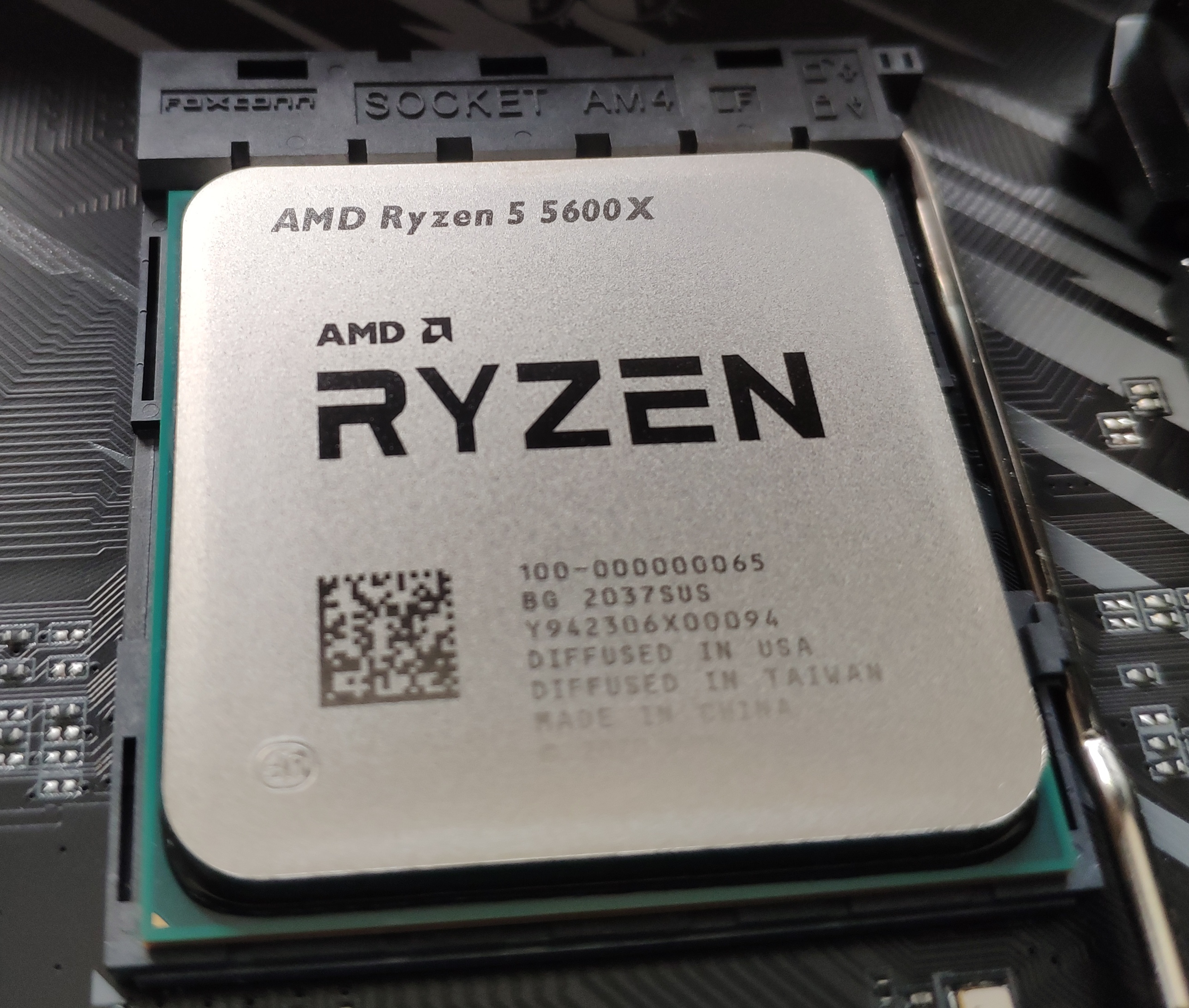 |
AMD Ryzen 5 5600X - 2020 If you arrived here from a Google search, for a Ryzen 5000/Vermeer machine crashing with Core Performance Boost enabled, you have a faulty CPU. Core Performance Boost is not overclocking and it is the CPU running within specification. This was a problem with early model Vermeer, more on it later. AMD's Ryzen 5000 series were "Zen 3". The Zen generation was the Ryzen 1000 ("Zen"), Ryzen 2000 ("Zen+"), Ryzen 3000 ("Zen 2") and this, Zen 3. The numbering skipped "4000" to align with mobile, which had begun its numbering a generation before Zen was released. AMD then immediately screwed up the naming again and re-released Zen 2 parts as part of the 7000 series, because of course it did. This entry will not cover AMD's chiplet design, nor its use of multiple foundries and a global supply chain. It will focus on this single CPU SoC (that's system-on-chip). In 2020, I was about ready for a main system upgrade, a Core i5-3570K was really, really, really long in the tooth so I set a budget and started designing the replacement system. Some parts could be replaced piecemeal, such as the case (Lian-Li LanCool II) and the video card (RX 570 8GB), and they were in 2019 and early 2020. The design settled on was an Asus X570-PRIME motherboard and a Ryzen 7 3700X. In 2020, AMD decided to bump prices. The "7" position in the market was more or less abandoned, so the Matisse refresh launch in July had a Ryzen 5 3600XT, a Ryzen 7 3800XT and a Ryzen 9 3900XT with a huge price difference between the 3600XT and 3800XT, more than enough to park a 3700XT in, but deliberately left empty. Apple's iPhone 6, for example, was another example of this strategy: The barely capable 16 GB model was much, much lower in price than the 128 and 256 GB models. It encourages people to move up to the next band: More people who would have bought a "7" will go to the "8" or "9" than will go to the "6". I went to the "6"! The unified CCX (a CCX in Zen/+/2 was two blocks of four cores) brought performance benefits, and many incremental improvements across the die also brought benefits. The 8 core, 32 MB L3 cache CC chiplet, two cores disabled in this 5600X, was a generational step above anything else on the market. It was a new architecture on the same process, featuring larger integer scheduler, larger physical register file, wider issue, larger reorder buffer, 50% wider FPU dispatch and FMA operations one cycle faster. It's a similar generational improvement as Haswell to Skylake was: "More of the same". AMD's Zen 3 lineup was made up of Vermeer and Cezanne, very similar to previous generations (e.g. Matisse and Renoir in Zen 2). Vermeer was chiplet based (and used an identical I/O die to Matisse) with a core complex (CCX) of 8 Zen 3 cores, each with two blocks of 2x1 MB L3 cache, so 4 MB L3 per core as manufactured, but each core has equal access to the entire 32 MB pool of L3. If one or more cores are disabled, its associated L3 cache is not. Vermeer does not have any graphics capability.
Additional retail launches in early April 2022 rounded out the series, adding a 5700X (de-clocked 5800X) and a 5600 (de-clocked 5600X). The star of the show, however, was always the launch of the 5800X3D in late April 2022, when AMD's internal game testing of dies intended for EPYC 7000X series CPUs found they wiped the floor with everything, in everything. One of the things to call out, however, is that these were GPU limited, all of them, on an RTX 3090, the fastest GPU available at the time. If all you wanted was gaming performance, a 5600X would get you everything a 5950X would in the most demanding games of the day, even at 1080p resolutions where load on the GPU is lighter. They were beating everything on release, though that was really only Intel's 11th gen which... well... 10th gen beat it too. 12th gen Intel did catch up, so AMD decided it was going to not just take back an undisputed lead, it was going to create a legend. This will be moved to a 5800X3D section if one ever arrives. The 5800X3D was never meant to exist, the 3D V-Cache was always supposed to be for EPYC 7000X-series server CPUs and it was designed for them, so servers with very good cooling, running at low clocks. The highest boost clock on any EPYC 7000X was the 7473X, which boosted to 3.7 GHz, could run at comfortably low voltages, and had only three cores per 8-core CCX active! The EPYC 7473X had eight CCXs with three cores per CCX active, so ran 24 cores and had 40 cores disabled, enabling only three cores to have the 32 MB on-die cache and the 64 MB V-cache all to themselves. Each CCX had 30 watts of the TDP available to it, meaning each core could average 10 watts. At a peak of 3.7 GHz, Zen3 would typically use less than 7 watts per core. The 5800X3D ran all eight cores of a CCX enabled and fit them into a 105 W envelope, allowing 13 watts per core to push the boost up to 4.5 GHz, which was important for games. This then meant AMD had to "take the X away", and limited the 5800X3D's overclocking. The V-Cache was never meant to run that fast, it was made for sub-4 GHz EPYC processors. It was also never meant to run very hot, the EPYCs would usually, even under full load, have a CCX temperature below 60C. A 5800X3D was far and away superior to everything else on the market in practically every game. A third of the price of a 12900K (or 13900K) and it'd beat them. Sometimes by a lot. It was absolutely legendary. All these were Zen3 CCX based SKUs, each with an I/O die (the same one as Matisse for the desktop parts), but later AMD made a monolithic "Cezanne", which cut off the second 2x1 MB L3 cache block (looking at the architecture, it's probably better to say Vermeer adds it, rather than Cezanne removes it), giving 2 MB L3 cache per core, twice that of Renoir, but keeps almost exactly the same GPU layout, 8 NCE/GFX9 GPU units, as "Radeon Vega 8" if fully enabled. The launch of Vermeer was not a happy one. Early models, including this one, appear to have been faulty, but as of time of writing this is still developing. AGESA updates made some settings more or less reliable, mostly more, but this 5600X could not run with Core Performance Boost (Analogous to Intel's TurboBoost), Memory XMP, or Precision Boost Overdrive enabled in AGESA 1.1.0.0 D or earlier... This may have been overly-aggressive binning. 5600X used dies which couldn't meet 5900X spec, so if it was a 6-core die and it was any good, it went in a 5900X. AMD appears to have been dramatically unable to meet demand for the 5800X and 5900X. In 2023, a similar issue appeared with early Ryzen 9 7950X3D samples, Linus Tech Tips came across one which showed many of the same symptoms these early Vermeers did in 2020. After the release of AGESA 1.2.0.0 in January 2021, which was meant to fix this issue for most people, didn't fix it for this CPU, it appeared this CPU was just worse affected than most others. Production codes later than around 2047 (week 47, 2020) were unaffected completely. The CPU was RMAed, the retailer confirmed it faulty, the replacement arrived and worked first time. This represented the first CPU in my experience ever faulty from the factory. Just to clear up some misconception online: Core Performance Boost is not overclocking. AMD specifies a maximum frequency of 4.6 GHz for Ryzen 5 5600X and Core Performance Boost needs to be enabled to get there. PBO is overclocking and not guaranteed to work or remain stable, but CBP is not overclocking and it is guaranteed to work. Also contrary to some more inaccuracy, CPB does not allow a CPU to run faster than its rated frequency. It allows it to run faster than its base frequency up to its rated frequency. For a Ryzen 5 5600X, base frequency is 3.7 GHz, rated is 4.6 GHz. If it doesn't do this, you have a faulty CPU. The confusion above comes from AMD's confusing naming. "Core Performance Boost" is used in BIOS for what AMD calls "Precision Boost", to avoid confusion with "Precision Boost Overdrive". One of those is not overclocking, the other is. What, then, actually is overclocking (as defined by behaviour which the manufacturer's warranty will not stand behind)? PBO or PBO2 is. Raising or lowering the TDP (or package power tracking) is not overclocking. Lowering the thermal limit below 95C is not overclocking, but raising it above 95C is. Running RAM faster than DDR4-3200 (including using XMP) is overclocking. Manually adjusting core voltage at all is overclocking, including offsets or Curve Optimizer. Manually setting static clocks to any frequency above base (3.7 GHz in this case) is overclocking. Essentially, overclocking is running the CPU outside of specification. For the Ryzen 5 5600X, this specification is Tjmax 95°C, DDR4-3200, maximum all-core 3.7 GHz, maximum boost 4.6 GHz, and core voltages 1.2-1.4 V (non-PBO boost adjustments excluded), although core voltages are less tightly defined by AMD.
| ||||||||||||||||||||||||||||||||||||||||||||||||||||||||||||||||||||||||||||||||
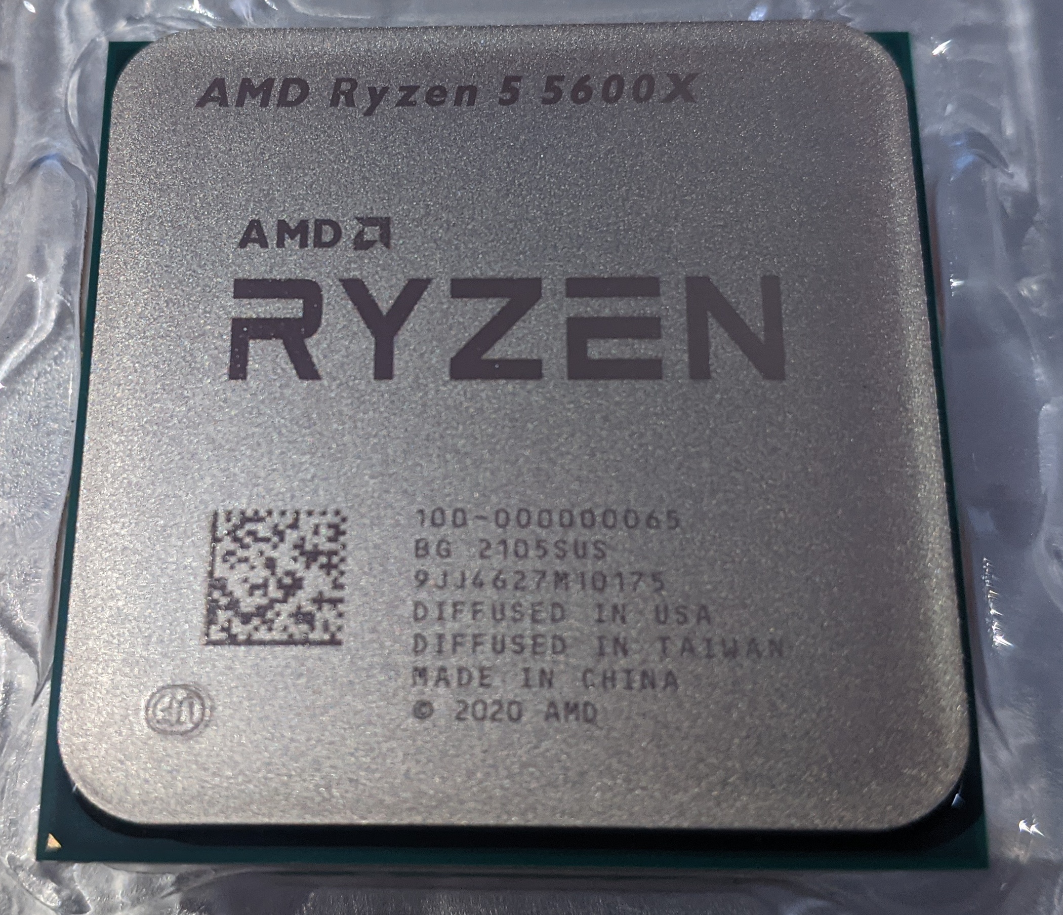 |
AMD Ryzen 5 5600X - 2020 An RMA replacement for the one above. This was the very first CPU I've ever had dead on arrival (DOA). I've had DOA motherboards, HDDs, RAM, you name it. Until that week 37 Ryzen, never a CPU. Before about week 47 2020, AMD Vermeer (Zen 3 chiplets) had some manner of issue with either the Infinity Fabric or the I/O chiplet, where if Core Performance Boost or Precision Boost Overdrive was enabled, the system was unstable. You'd think "Aha, no, that's the core complex chiplet, not the I/O!" However, enabling XMP to run RAM at 3200 MHz was an instant crash, on RAM known to be good. Some people reported adjusting various I/O chiplet and Infinity Fabric related voltages alleviated the issues, others found that AGESA 1.2.0.0 fixed it. Still others could not achieve stability in any circumstances, such as the one above. It was clear that AMD was working on Vermeer's stability in AGESA code, so was aware of an issue, but successfully managed to keep it quiet. It wasn't a dog by any means. With relaxed limits and Precision Boost Overdrive enabled, Cinebench R20 scored 4,512 and R23 scored 11,724, for example as all-core workloads, but this is about what it should score with just default tuning. That it needs encouragement to go that far isn't great for this CPU, but it is great in general: Precision Boost Overdrive will get the CPU's peak performance, or very close to it, straight out of the box. If you have a worse CPU than normal, it'll still get you as much has it can. Only if you have a far better CPU than normal (you don't, they all went into the Ryzen 9s!) will PBO leave performance on the table. Utilities like CTR or Project Hydra were able to estimate CCD binning quality, they'd consider it based on energy efficiency, and rate from Bronze, through Silver, Gold, to Platinum. Of course this was rated "Bronze" with an energy efficiency given as 3.78. As these utilities are able to get every last scrap of performance out of Zen 2 and Zen 3, a performance ranking could be given. Coupled with AGESA 1.2.0.6+ (which reduced performance!!!), this 5600X ranked around 95% of a typical 5600X! This chip hard lost the silicon lottery. This particular Vermeer was manufactured in week 5 of 2021, where Ryzen 5 5600X was the lowest SKU AMD had and it was stockpiling poorer bins to launch later as 5600 (just as Cezanne became the unlovable 5500). The better bins of the 6-core Vermeer all went in the Ryzen 9 5900X, which used two of them and rated them for 4.8 GHz boost, so needed better silicon. Why throw away good silicon in the 5600X when it could go in a 5900X? I also want to clear up another inaccuracy here: There were no 4+8 5900X SKUs. Every last one was a 6+6 CCD layout. An asymmetric core layout (which AMD has done before) would cause L3 cache balance to be different between the two CCDs, the 4 core CCD would have the same 32 MB L3 cache as the 8 core CCD, but half the number of cores sharing it, so would run a tiny bit faster. However, demand was high, so anything that could meet 5600X's 4.6 GHz single core boost and maintain all core at 3.7 GHz base, but didn't quite meet the specification for a 5900X, was going out of the door as a 5600X. What do you do if you lose the silicon lottery? Undervolt. With a -0.054Vcore offset, power was reduced from 55 watts (CPU die only) to 43 watts under a Cinebench R23 load without any impact to performance. By early 2023, reports on 5600X binning and clock capabilities improved significantly, with many reaching 4.8 GHz or higher, which the earlier parts couldn't. The demand for very high end Ryzen 9s had evaporated, these people go for the fastest possible, which became the 7000 series, or Intel's newly-competitive later-2022 lineup, or the 5800X3D. The best non-Vcache CCDs could now be used in lower SKUs, typically 5800X, 5800, and 5700X (the 5800 and 5700X differed in how one was called 5800 and one was called 5700X!), meaning dies which would previously have been poor 5800X dies were now being used as 5600X dies. Back in 2020 and 2021, in normal, un-overclocked state, the single threaded performance on the Ryzen 5 5600X was extreme. It not only beat everything Intel could throw at it, but also everything else in the Vermeer-based stack, even the frighteningly expensive Ryzen 9 5950X. Cinebench R23 has the 5600X here at 1,581 single core... CPU power was being reported as, CCD + SoC, 13 watts. To underperform that, an Intel Core i5 10600K (Comet Lake) would use triple the power. Intel quickly pushed out the 11th generation Core series (Rocket Lake) and... to quote Steve from Gamers Nexus, they "were better off as sand on a beach somewhere". They regressed performance, sometimes significantly. Base clocks were down, core counts were down, power draw was off the scale. This particular one did best at curve optimiser -24, 0, -24, -24, -24, -11, identifying core 2 as particularly weak. With PBO platform limits set at 100 watt package power tracking, 120A TCD and 150A EDC, (10X scalar), it'd usually handle around 4,450-4500 MHz all-core in Cinebench at 83C. PBO is also temperature sensitive, a better cooler raised clocks by around 100 MHz, but then also exposed instability in core 2, meaning that had to be given a positive offset! As a demonstration of how far we've come, I ran some benchmarks against a dual-CPU, 12 core, 24 thread, Xeon E5-2640. The Xeons have 32,400 core-MHz, the Ryzen has 27,600, although boost and turbo does influence that. Xeon bandwidth is in triple-channel DDR3-1333 (they support quad, but I don't have enough registered ECC DIMMs) for a total of 2x 31.6 GB, the Ryzen has dual channel DDR4-3200 for 51.2 GB/s. This makes bandwidth per-core 5.2 GB/s for Xeons and 8.5 GB/s for the Ryzen.
While this isn't a sound and robust suite of benchmarks, they do generally agree with each other and there are no major upsets, other than Ryzen's hardware AES support. We're probably selling the Ryzen short here, since highly threaded workloads are what the Xeons were designed for, and the Ryzen excels with fewer threads. The mid-range Ryzen isn't just able to match the HEDT Xeons of eight years earlier, it beats them soundly. That said, the Xeons put in such a good showing that they'd be competitive with a first or second generation Ryzen, such as a Ryzen 2700X... Or, indeed, with most of Intel's 8th-11th generation. This particular Ryzen 5 5600X was significantly underperforming, even with PBO overclocking enabled. A quick comparison (in July 2023) gave results of:
These results are on a later AGESA version to the Xeon comparison above, the AGESA 1.2.0.5 and up reduced performance quite a bit in all-core workloads for some parts, typically those with weaker cores. The competition to Ryzen 5 5600X was Core i5-11400. Raw specifications looked similar:
What did the extra $3 and the much more expensive platform (around $60 more) get you on Intel's side? It got you 80% of the performance of the 5600X. No, not a typo. You'd pay $60-$100 more and get around a speed grade worse. Intel's real response was Alder Lake, a year later, which delivered Intel's largest single generation bump in performance in over five years. The i5-12500 (at $212) more or less ran evenly with the 5600X, at around double the power. Intel was now definitely on the back foot.
| ||||||||||||||||||||||||||||||||||||||||||||||||||||||||||||||||||||||||||||||||
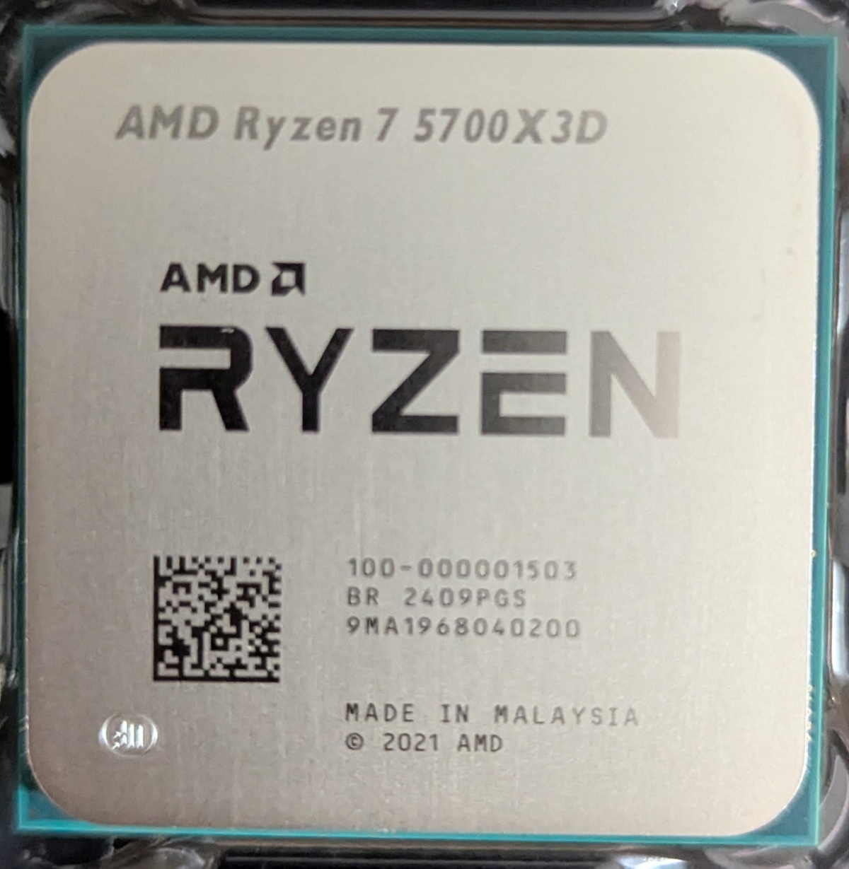 |
AMD Ryzen 7 5700X3D - 2023 The first use of AMD's 3D V-cache was Milan-X, some EPYC CPUs, based on Zen 3 (Milan and Vermeer were the same silicon) but with the EPYC I/O die for much, much greater I/O performance. Of course AMD engineers toyed around with silicon in their test labs and one of them noticed Milan-X was way more effective in game benchmarks than expected. All Vermeer/Milan core complex dies (CCDs) had the through-silicon vias to connect to stacked L3 cache, it was just simpler to design that way and if the CCD went on a big substrate with a "Rome" I/O die (from Zen 2 EPYC) it was an Milan EPYC. If the CCD went on a smaller substrate with a "Matisse" I/O die (from Zen 2 Ryzen), it was a Vermeer Ryzen. If it had the 3D V-cache (a 64 MB high performance SRAM), it was "-X". So, AMD had some Ryzens made up with the Vermeer-X. In testing, they could clock much faster than AMD had anticipated, the design was meant for sub-4 GHz operation, but AMD had them running north of 4.4 GHz fairly easily. At these kinds of clocks, while fairly low by desktop standards, Vermeer-X was absolutely smashing anything and everything in gaming performance. AMD got enough of them made for a commercial release and launched the Ryzen 7 5800X3D in April 2022. It ran at a maximum of 4.5 GHz and overclocking was locked out on it. Clearly, many Vermeer-X CCDs wouldn't actually run that fast and, complicating things, AMD launched AM5 not long later. The demand for the king of AM4 evaporated when AM5's low end was doing just as well: The Ryzen 5 7600X could usually beat a 5800X3D (though not in 1% lows). While demand for the 5800X3D remained steady, AMD was accumulating a lot of "-X" dies which weren't able to reach 4.5 GHz reliably. So, in January 2024, AMD released the Ryzen 7 5700X3D. This was rated only to 4.1 GHz and, typically, would run at 4.0 GHz in most workloads. Many, many more Vermeer-X dies were able to do this and AMD's launch price of £240 (UK) or $250 (US) reflected that. By July 2024, price had fallen to £210 in the UK and, in most of early 2025, was hovering between £200 and £210. Including all relevant taxes, this cost me £209 in mid-June 2025. AMD had discontinued the 5800X3D in October 2024 and a limited launch of the 5600X3D had dried up parts of the stock, while the 5700X3D remained available until it, too, was discontinued in August 2025 having had retail availability for only 18 months. Synthetic benchmarks were not where the 5700X3D shined brightest, they typically didn't really notice the 96 MB L3 cache. Clock for clock, FFMPEG doing HEVC/H.265 encoding was faster, but we don't have a clock for clock comparison here... X3D costs us clock to get! A 5800X (same 8 cores, 4.7 GHz) was £40 cheaper than the 5700X3D, while a 5900X (12 cores, 4.8 GHz) was £15 more expensive: Both would smash the 5700X3D in this kind of workload. By a lot. X3Ds were for games. In Baldur's Gate 3, the 5700X3D beat the entire AM5 lineup before the 7800X3D was released. BG3 was a bit of an extreme example, it performed badly on non-X3D AMD CPUs and even a crappy little Intel i5-13600 could beat AMD's stack. In most games, it performed next to a 7600X, which wasn't at all bad for a CPU which had a 1.3 GHz clock disadvantage and would use substantially less power.
| ||||||||||||||||||||||||||||||||||||||||||||||||||||||||||||||||||||||||||||||||
| Raptor Lake |
Could it get any worse for Intel? In late 2022, Intel released Raptor Lake, the much-anticipated successor to Alder Lake. Rocket Lake, which debuted Intel's new microarchitecture (as Cypress Cove), had back-ported the Sunny Cove architecture from 10 nm to 14 nm, since Intel still hadn't got 10 nm commercially scaling. In Rocket Lake, it was a huge disappointment and usually slower than the Coffee Lake CPUs it replaced. Alder Lake straightened up most of that and Intel's 12th generation Core products were finally back able to compete with AMD. Eyes were on 13th generation as Raptor Lake. AMD had pulled a blinder with the Ryzen 7 5800X3D and everyone wanted to see what Intel's response was. Power usage was off the charts, while TDPs were reasonable, actual power use could top 250 watts, but that's fine. Just use a big tower cooler or AIO cooler, whatever. Power usage was through the roof, but Raptor Lake was not beating AMD. In most cases the 5800X3D remained on top, and AMD's Zen 4-based 7800X3D was more or less untouchable - AMD had dropped the AM5 paltform a month earlier. Okay, so Intel was behind, but that happens. No big deal. Throughout 2023 a pattern of unstable Raptor Lake systems emerged. One game development studio said more than half its Raptor Lake workstations were unstable. Unreal Engine 4 and Unreal Engine 5 games using the Rad Game Tools texture compression library (very common) would display an "Out of Video Memory" error. What had actually happened was the texture processing on the CPU had produced an error, the texture could not be uploaded to VRAM since it didn't exist, but Unreal Engine saw that the texture load had failed, so it had to be out of VRAM - When it was not. Intel then could not have handled the issue worse. It adopted DARVO tactics! It first denied there was any problem and failure rates were not elevated at all. Then, it attacked the media and others in the PC ecosystem, with Nvidia famously dropping an bomb in the release notes for driver 552.12 linking it to Intel. Then Intel reversed the victim and offender, blaming bad motherboard defaults, as though Intel hadn't controlled motherboard behaviour for decades. Only when Intel had ran out of excuses did it acknowledge there was a problem. As though DARVO wasn't bad enough, Intel now sought to minimise the problem. It was only affecting -K versions, the unlocked CPUs, was the first claim. More proof came out of it affecting laptops, which never have -K CPUs, and desktops not using -Ks. Then it was "13600 or 14600 and up"... Nope, we saw i3s being affected too. Intel released microcode update after microcode update to try to get to the bottom of it and, finally, in August 2024, released a microcode which should have fixed it. For already damaged CPUs, there was no fix, however. This fix was revised in September as microcode 0x12B and is the minimum version which will not destroy the CPU. Intel revealed that a clock tree was being run at an inappropriate voltage for its temperature. At high temperatures, which modern CPUs are designed to run at, voltage has to be reduced to avoid degradation. The reduction in voltage then reduces the maximum attainable clock, so there's pressure to run the voltage as close to the threshold as possible: Intel went over the threshold. Ultimately all Raptor Lake CPUs were affected, except the very few which were really the older Alder Lake being dressed up to pretend they weren't. Intel could not have handled this any worse. By trying to blame the motherboards, it was contradicting its own previous statements which said the PL2 limits were "within spec". Ultimately Intel had to give a two year warranty extension to affected processors, but it did successfully avoid a recall. |
||||||||||||||||||||||||||||||||||||||||||||||||||||||||||||||||||||||||||||||||
| Overclocking? What's that? |
In the olden days, CPUs were run quite simply as fast as they would pass validation. All 386s needed a 5V power supply, so the voltage wasn't a variable, and they just were binned as they ran. Later, Intel started to down-bin chips. By the late 486 era, Intel had got very good at making 486s and everything it churned out would hit 66 MHz easily, but this would have caused a glut of 66 MHz parts: The market still demanded slower and cheaper chips, as well as faster and more expensive ones. If Intel was to simply sell everything at 66 MHz, then Cyrix and AMD would be more than happy to undercut Intel dramatically with 50, 40 and 33 MHz processors, subsidised by faster and more expensive 66 and 80 MHz chips. Similarly, by the Pentium-MMX days (about 1996 or so), everything Intel sold was capable of running 200-250 MHz, but Intel was still selling parts rated for 150, 166 and 180 MHz. It was nothing to buy a Pentium 166-MMX and run it at 233MHz. Many overclockers cut their teeth on a Celeron 300A, in 1998, which would overclock really easily to 450 MHz, giving massive performance improvements. This kind of overclocking, taking a deliberately de-rated product and restoring it to where it "should" be was to be repeated time and again, the Athlon XP 2500+ was a de-rated 3200+, the Pentium 4 1.6A would easily be set up to run at 2.13 GHz just by setting a 533 MT/s bus and would usually go a lot further than that. The pattern repeated itself time and again, low clocked CPUs could very often be overclocked explosively. AMD Opteron 146 and 165 were popular, while sold at 2.0 and 1.8 GHz respectively, it didn't take much to get them going at 2.8 GHz. Intel's Core 2 Duos were almost universally capable of 3.2 GHz, later Intel's Core i5 2500K became legendary for being able to hit very high clocks, from a base clock of 3.3 GHz it would often pass 4.0 with ease. Most of them found a nice happy place between 4.2 and 4.4 GHz. |
||||||||||||||||||||||||||||||||||||||||||||||||||||||||||||||||||||||||||||||||
| Cancelled Maybes, Also-Rans, and Interesting Dispatches From The Front | AMD X3D AMD's 3D V-Cache was a feature of its EPYC 7000X datacentre processors, such as the EPYC 7773X. The huge L3 cache here, 96 MB per Core Complex Die (the Milan CCD die was termed "Milan-X"), greatly improved database and scientific processing. In things like computational fluid dynamics, the huge L3 cache as much as doubled performance. Milan-X had 32 MB on the CCD and 64 MB affixed to the top of it and was always mounted as eight CCDs with two large quad-channel I/O dies. AMD positioned them like so.
Anyway, AMD's product labs got some Milan-X CCDs and mounted them with a Matisse I/O die on a hunch they might do pretty well in games, so forming Vermeer-X ("Vermeer" is the consumer-level name for the Zen3 CCD, "Milan" is the datacenter name, they're identical). Vermeer-X was explosively good in games! However, the TDP of EPYC was 280 watts across eight CCDs, giving each CCD only 35 watts if running flat out (they'd use more if other CCDs weren't) while desktop parts typically ran higher clocks (4.5-4.8 GHz in Zen3) and used much more power, triple the power of EPYC, to maybe 100 watts per CCD or even more. This led to a weird binning situation. CCDs able to run at lower voltages and lower powers became destined for EPYC, but these were usually the same silicon able to run at very high clocks. Silicon with a few defective cores didn't matter for EPYC, of course, the 7373X disabled 75% of all the cores anyway! For a powerful gaming part, and AMD was looking at something able to beat the entire rest of the market, eight cores was necessary, all working at fairly high clocks. For known-good 8-core V-cached CCDs, the option was then one of them in a $400 5800X3D or eight of them in a $8,000 EPYC 7773X. Of course AMD wasn't about to sell hundreds of thousands of top end EPYCs with V-cache. For most cloud hosts, the regular EPYCs were plenty. However, what if AMD could sell hundreds of thousands of V-cache equipped dies? The bigger the order from TSMC, especially for the 3DFabric SoIC (AMD was using CoW, "Chip on Wafer") chip stacking TSMC was hotly billing, the lower the cost per part would be, and so the higher the margin on the big EPYCs. The economics must have worked out right, becuase AMD launched the 5800X3D and, much later, a few less capable parts as 5600X3D in a limited edition. Phenom II X8 There were seemingly samples out there, and they were named Phenom II X8 "XY20", where "XY" was the clock speed. There was the base model 2420 (2.4 GHz) up to the top end 3020 (3.0 GHz) making two stops at 2.5 and 2.8 GHz. Valid production codes leaked out, via Jetway's HA18 motherboard's CPU support list and ECS' A890GXM-A2 motherboard's CPU support list.
On 32 nm, a Llano core was 9.69 mm² excluding the L2 cache. Stars allowed 256 kB, 512 kB or 1024 kB L2 cache. It could possibly have had 2048 kB L2 cache, but would have had to raise cache latencies and AMD seemed unwilling to do this. Assuming the same L3 cache, an "X8" would have been 1,050 million transistors, actually smaller than Llano's 1,178 million. If we use Zambezi's (AMD FX) 3.8 million transistors per mm², this would have been 309 mm². If we use Llano's density (same cores, but that dense GPU and dense caches) it would have been 230 mm². From a look at the die floorplan, the Stars cores in Llano take up 55% of the die area, so use 125.4 mm². Dumbly doubling them gets a 250.8 mm² die with no L3 cache. This means we're in the right ballpark with our calculations based on Zambezi above, and 309 mm² is likely fairly accurate. This would be a very large CPU die, and would need a full product stack to make it economical. We can also take something else away from the Llano synth: A quad core non-IGP Llano was still rated to 100 watts at 3 GHz. This actually makes it less power efficient than the 45 nm Stars cores! At higher clocks (and by higher, we mean anything north of 2.7 GHz), Llano was worryingly inefficient. The 8T-SRAM was not efficient, GloFo 32nm was not great, and the VLIW-4 GPU was very power hungry. Finally, the Stars architecture was not designed at all with efficiency in mind, its key efficiency feature, independent core clocking, was disabled by AMD as Windows couldn't handle it very well. An 8-core Phenom II X8 on 32 nm would have either been competing with AMD's Bulldozer architecture (and would likely have beat it) or with AMD's lower end Llano architecture, which it was too big and expensive for. It's conceivable that AMD wanted the X8 "ready to go" in case something very bad happened with the launch of Zambezi/Bulldozer, AMD already knew performance wasn't great with Bulldozer. 10 GHz by 2004 Intel's 2001 promise to hit 10 GHz in the next few years (this was based on critical-path optimisation and Dennard Scaling) evaporated quite spectacularly with Prescott in 2004. A successor, Cedar Mill (65 nm) appeared, didn't run much faster (it was a direct die-shrink) and was still a 31 stage pipeline. Tejas, the successor to Cedar Mill, was taped out and tested by the end of 2003. It had a 40-50 stage pipeline and ran as high as 7 GHz. The testing parts ran at 2.8 GHz and 150 watts. A full-on 5 GHz Tejas would have needed nearly 300 watts. Intel insiders told me at the time that they had LN2 cooled Tejas parts running at 7.2 GHz quite stable. Trouble was, they used 320 watts and were about 30% faster than the already terrifyingly fast Athlon64 FX-51 (which used about 70 watts). In May 2004, Intel announced that Tejas was to be cancelled. The era of Dennard Scaling was over. Moore's Law, which was partly based on Dennard Scaling, but also based on economics, would die in around 2018-2020. AMD's K7 Codenames There's quite a lot of misinformation out there around this, so here we'll set the record straight. The original Athlon with off-die L2 cache on the 250 nm process was codenamed "Argon", the original 500-700 MHz parts. AMD then went all astronomical: "Pluto" (550-800 MHz) and "Orion" (900-1000 MHz). Pluto was so named as its cache divisor was 2:5 (L2 cache ran at two clocks for every five clocks of the core) but was seemingly originally meant to be 2:3 (so a 750 MHz Athlon would run 500 MHz L2 cache instead of the 300 MHz it was limited to), so is thought to be a nod to the then-planet Pluto's orbital resonance with Neptune, which is a 2:3 resonance. Orion got its name from the 1:3 cache divisor. The constellation Orion is famous for its three stars asterism of "Orion's Belt". As a side note, it appears AMD was indeed expecting 500 MHz-capable synchronous SRAM to become available at prices it could justify by the time Pluto was needed, but the GHz-race took off and aside from this the demand for synchronous SRAM never materialised. Next came Thunderbird, Mustang, Spitfire, and Camaro. Mustang and Camaro were never released, but Thunderbird became the first Socket-A Athlon. Camaro was a Palomino-based Duron, which was renamed to "Morgan" to fit in with the horse breed theme. and Spitfire was the first Socket-A Duron. These were not meant to be named for horse breeds, but instead classic American cars. Rumour is that Detroit got wind of this and was famously litigous in trademark law, so AMD decided it could also name them for horses. Palomino (180 nm) became the Athlon-XP, Appaloosa was unreleased. Appalbred/Applebred became a thing! Thoroughbred was the 130 nm shrink of Palomino. So did Barton (130 nm), named for Sir Barton, the first horse to win the American Triple Crown. Thorton was also a thing, sold as Athlon-XP. What was going on? Well, AMD cancelled Appaloosa, a Palomino-based Duron with only 64 kB L2 cache and instead cut down the L2 cache of some Thoroughbreds to make a virtual Appaloosa from Thoroughbred. This "hybrid" was therefore named "Appalbred", which was often misquoted, even by AMD themselves, as "Applebred". AMD did similar with "Thorton". Cutting down Barton's 512 kB L2 cache to 256 kB essentially turned it into a version of Thoroughbred. So Thorton and Appalbred were one CPU core pretending to be another, even if, in Appalbred's case, the other was never released. Athlon "Mustang" In 1999, AMD revealed they were kicking around different K7 SKUs, the names "Athlon Professional" and "Athlon Select" were mentioned for high-end and entry-level parts. "Select" became the Duron, while "Professional" was never released, but what was it? The MHz race to 1,000 MHz went a bit faster than anyone, even AMD, had anticipated. AMD was preparing a 50-60 million transistor successor to the original K7, by integrating L2 cache, expanding SSE support to full, and adding a hardware prefetch system. This was called "Thunderbird" and it was going to go "Xeon-like" with a workstation/server class variant with 1 MB L2 cache named "Mustang". As things worked out, however, "Thunderbird" was not ready but Athlon could not scale past 1 GHz due to its off-due L2 cache being limited to just 350 MHz. "Thunderbird" became "Palomino" and a very easy validation of the unchanged Athlon with 256 kB of on-die L2 cache was released as "Thunderbird". "Palomino" debuted as "Athlon4" in small quantities as mobile parts, later as "Athlon XP", but AMD's original intention was to go straight from the cartridge-based Athlon to what eventually was released as Athlon XP. This would have been an awesome bump in performance and would have probably buried the Pentium4 before it had ever had chance. So what of Mustang? A 1 GHz sample of a Thunderbird (no enhancements) with 1 MB cache which leaked out turned out to be maybe 10% faster than an equivalent Thunderbird - Palomino would have been faster than Mustang. As we found later with Barton, which was maybe 5% faster with 512 kB cache instead of 256 kB over Athlon XP, the K7 core wanted faster cache, not more of it. Palomino's prefetcher made the cache look faster, so gave the core a large performance boost. The Athlon Backup Plan What, though, if Athlon had failed or been delayed? AMD had another trick up its sleeve, another revision of the venerable K6. At 180 nm, the AMD K6-2+ had 128 kB of L2 cache onboard, the K6-III had 256 kB. While they had short pipelines and couldn't clock highly, they were somewhat present in the retail channel and enthusiasts reported success in hitting as much as 650 MHz with them. They were highly competitive with Intel's Celerons, but unnecessary: AMD's Durons were utterly destroying Intel's low-end. It got so bad that Intel contractually forced OEMs to buy Celerons, one OEM anonymously complaining that Intel was refusing to guarantee Pentium III-E supply unless they also committed to a minimum Celeron order! This kind of "buy our low end if you want our high end" stunt didn't die there. Nvidia was heavy on it in the RTX 2000, 3000, and 4000 days. The reason so many prebuilts had wildly inappropriate RTX 4060s was because Nvidia demanded "fractional ordering", so maybe 10 4060s to 4 4070s to 2 4080s to 1 4090. Actual numbers were nearly impossible to find due to confidentiality clauses. In any case, the OEM had piles of the low end it needed to get rid of any way it could. SIMD comes to x86 SIMD allows a single instruction to work on two, four or eight pieces of data at the same time. The instruction and data are loaded normally, but the data is in a packed format: A 128 bit MMX/SSEx value is actually four 32 bit values concatenated. The same instruction works on all four values at once. This is very cheap to implement, as the instruction setup and transit logic can be shared, while only the ALUs or FPUs need duplication and they're small without their supporting logic. By 1995, Intel engineers and architectural designers wanted to add SIMD to the next CPU core, P6. Intel management was more conservative, however, as adding a new instruction set and register aliasing meant a new CPU mode. Could it be done by modifying the existing P5, and in a way it wouldn't be so intrusive? It could be, and a very limited form of SIMD which worked on integer data formats only was added to P5 and named "MMX". It did very little and had extremely limited use: It could be used to accelerate the inverse discrete cosine transform stage of DVD decoding (and the discrete cosine transform step of MPEG1/2/4 encoding), but very little else showed any benefit. What was originally proposed eventually became SSE, released with the PentiumIII in 1999. Had Intel been that little more aventurous, MMX could easily have been something like AMD's "3DNow!" which added SIMD as an extension to MMX itself, making MMX much more useful for real-world applications and allowing it to do floating point add/sub/mul/reciprocal and so on. Performance of 3DNow! implementations of code which even a fast P6 FPU would choke on were very fast. 3DNow! ultimately failed as Intel never adopted it. Some game engines supported it, DirectX also did, and on Athlon and AthlonXP. AthlonXP added in 19 new instructions which were part of SSE working on integer data. As 3DNow! was aliased onto the x87 registers, it could be saved and restored using conventional FSAVE and FRSTOR instructions, meaning the OS need not support 3DNow! at all for code to be able to use it. AMD continued 3DNow! support until ending it with the Bulldozer architecure on laptop, desktop and server, and no AMD ultra-mobile core has ever supported it (Bobcat didn't have it). 3DNow! prefetch instructions (PREFETCH and PREFETCHW), which remain a really good way to prefetch in certain situations, remain supported and even Intel implemented them in its Atom processors (Bay Trail onward) and Pentium4 processors (Cedar Mill onward) and PREFETCHW became mandatory for Windows 8.1 and up. The most recent APU supporting 3DNow! is Llano, which is based on the Phenom-II era "Stars" core and has a VLIW-4 based TeraScale3 GPU integrated. What the heck was Bulldozer? Instead of triple back end execution resources as seen in K7, K8 and K10, why not have narrower, faster, double back ends? Surely 2x2 running at 5 GHz would be better than 1x3 running at 3.5 GHz. Bulldozer beefed up the FPU, but didn't duplicate it. It slimmed down the ALUs from 3x ALU and 3x AGU to 2x ALU and 2x AGU (AGUs are a sort of housekeeping unit, they free up ALUs from having to calculate memory addresses), but each module had two distinct and independent integer units. Would 2x2 beat 1x3? No! No it would not. Maximum per-clock single threaded performance, still very important in 2011, was around two thirds that of Phenom II (K10), which was already significantly lagging behind Intel. Each core was only two units wide! Intel's Sandy Bridge enjoyed a 40-50% lead over Bulldozer, as the AMD FX-8150, and used less power to do so. If lots of threads were available, such as in heavy video encoding or synthetic benchmarks, Bulldozer could sometimes use its clock speed advantage to sneak a very narrow win. Where many threads were not available, Bulldozer was slower, often lots slower, than the previous generation. The question remains, however, why was Bulldozer so slow? It had no right to be! Clustered multiprocessing was a good idea and Bulldozer's architecture in many places was obviously transitional between K10 and Zen. The branch prediction unit, front end and decoder, the tag-indexed physical register file for OoOE is identical to Zen, the FPUs are the same as Bulldozer, but now 128 bits wide and the ports were tweaked). Just looking at Bulldozer's architecture reveals a CPU on roughly the Sandy Bridge or Haswell technology level, and it should perform like them. Why, despite being so much more advanced in every way, did it underperform K10 at the same clock? This table will explain everything.
Now do we understand why Bulldozer failed so hard? A L1 cache miss is an absolute disaster for performance on any CPU, and Bulldozer, as the Athlon X4 880K's "Excavator" derivative, had just 16 kB L1 data cache, shared between two modules. This was a quarter of K10 (Phenom II X4) and half Ivy Bridge (i5-3570K). Even in the easily cached 7-Zip benchmark, which both other CPUs exceed 99% hit-rate on, Bulldozer manages only 97%. Even if the L1 miss results in a L2 hit, that three clocks of waiting has become four times as impactful and Bulldozer didn't have enough parallelism to hide that latency. To be fair on it, nothing back then did. This is what sank Bulldozer. In Hot Chips presentations, first Bulldozer was presented with 64 kB L1 cache, then with 32 kB a year later, then finally launched with 16 kB. AMD knew this was a problem, but had no way around it. AMD had moved from 6T-SRAM for L1 cache cells to the faster 8T-SRAM, then had layout problems with it. The curious reader is invited to read more over on Chips and Cheese. In short, Bulldozer laid the groundwork for Zen but suffered horribly itself for doing so. |
||||||||||||||||||||||||||||||||||||||||||||||||||||||||||||||||||||||||||||||||
| Process Nodes and Fabrication |
A process node is the "fineness" of the fabrication process, or how small a feature it can etch into the silicon, usually measured by "feature size", but not always. Gate length is another measure, and, by around 2013, the process node was simply a number and bore little relation to what was actually being fabricated. The measurement used today is the "half-pitch" of a DRAM cell, so the distance between two identical features of two adjacent DRAM cells. We started measuring them in microns (µm, micrometers, one millionth of a metre), so we had Pentium MMX fabricated ("fabbed") on a 0.35 micron process. The next process was a 0.25 µm (K6-2, Pentium-II), the one after was 0.18 µm, then 0.13 µm, 0.09 µm, 0.065 µm... we started to use nanometers then, so 130 nm, 90 nm, 65 nm, 45 nm, 22 nm, 20nm (at TSMC), then 14 and 16 nm in 2016. Samsung was shipping 7 nm in 2018, GlobalFoundries expected volume in early 2019, but Intel, always one step ahead of everyone else, royally screwed up its 10 nm process and was still stuck on 14 nm. There's a clear path to at least 4 nanometers according to Intel but at that point there are too few atoms across a gate to be able to actually hold a proper band-gap. The 14 nm node has just thirty silicon atoms across the gate (silicon's lattice constant is 0.543 nm). The semiconductor properties of silicon depend on its small band-gap, which depends on molecular orbitals, which require a large number of contributing atomic orbitals. Less than 30 and there aren't enough atomic orbitals to contribute, so the band-gap between bonding and antibonding orbitals is poorly defined. The width of the gate, that is, how much insulating material is between the two ends, was just 25 nm on the 65 nm bulk silicon process. As there were fewer than 100 atoms across the gate, leakage via quantum tunneling was significant, leading to higher power use. A typical contract fabrication would have two processes, low power (LP) and high performance (HP). The LP process would have a wide gate, maybe 50 nm, but poorer density as a result. As the distance between transistors affects how fast they can be switched (clock frequency), LP fabrication means the chip doesn't run as fast. HP has a narrower gate, so runs faster, but uses far more power. The gate's thickness was down to as little as 1.5 nm (Intel), meaning around three atoms of oxide insulated the switching part of the transistor: This causes massive leakage. By 22 nm, in 2012, the gate oxide layer was just 0.5 nm, about twice the diameter of a silicon atom, and could not get any smaller. Intel delayed 14nm from "the end of 2013" to the last quarter of 2014, a nearly-unprecedented year long delay to a process. Cracks were already showing, even this early, even before any 14 nm CPU had been marketed. The 22 nm process Haswell launched on had some refinements and tweaks, mostly for yield, backported from the 14 nm project. They were minor, but Haswell had far more die variability than Ivy Bridge did. If you bought an i5 3570K, you'd get a 4.2-4.4 GHz overclock out of it without really trying. This was practically guaranteed. Haswell dies, however, were all over the place. An i5-4570K might get you to 4.6 GHz, would usually get you to 4.4-4.5, but a worrying number, maybe two out of every five, wouldn't even go that far. Haswell die variability was very high, which is something you'd expect from a new, cutting-edge manufacturing process, not an old and proven one. Volume availability of 14nm was not until the middle of 2015, nearly two years after estimates, and Broadwell just a die shrink of the earlier Haswell, from 22 to 14 nm, a "tick" in the "tick-tock" model. Intel considered the 22 to 14 nm switch to be the most difficult it had ever done. Because Broadwell was so late, Skylake was ready to launch just a few months later. There weren't many desk Broadwell CPUs, the Core i7-5775C and Core i5-5675C were it. They did not offer anything Haswell didn't already do, but did experiment with 128 MB eDRAM for L4 cache. There were a trickle of HEDT CPUs a year later, in 2016, an entire line of mobile CPUs, and the Xeon E5 v4 series. 14 nm was refined many times, to a "14+++" for Comet Lake, but 10 nm was always slightly out of reach, not ready for prime time. Intel sampled 10 nm in 2018, but achieved mainstream availability only in 2020: In 2020, Intel launched the short-lived Tiger Lake which had some very limited products available, the desktops being denoted by a "B" in the 11th generation Core lineup. The rest of the industry was pushing 7 nm and even ramping up 5 nm. To be fair on Intel, its 14 nm class process had the best geometry in the industry, but did not match its leading geometry with leading density, which is the entire point! Intel, however, was still struggling to progress beyond 14 nm. Some very limited run 10 nm products had seen the light of day. Intel stretched the 14nm Skylake core through several "generations" of thoroughly similar chips, Skylake, Kaby Lake, Coffee Lake, Cannon Lake, Whiskey Lake and Comet Lake all of which used the same central architecture. Now, Intel was the worst victim of this, and fell the furthest, but the struggle below 20 nm was industry-wide. GlobalFoundries completely failed to make a working 14 nm, it licensed Samsung's 14LPP. TSMC initially sold its proces, a little less tight than Samsung or Intel's 14 nm, as a 16 nm. For the first time in living memory, Intel was not first to a major node, Samsung was. GlobalFoundries ceased R&D and was not persuing nodes below its optimised 14 nm, which it calls 12 nm. TSMC came out of it a winner. On 10 nm, Intel hit it out the park to begin with: A year after TSMC and Samsung, but almost twice their density! TSMC and Samsung hovered between 50 and 60 million transistors per square millimeter, Intel released 10 nm Cannon Lake with 100.8! Then failed to make it mass production. A single Cannon Lake, Core i3-8121U, was ever made. Its Gen 10 IGP was never enabled. That single SKU lasted just 1.5 years on Intel's availability list and sold extremely poorly. Who wanted a U-series CPU for an ultra-light, which had no graphics capability?! Two years later, another limited run, Tiger Lake. It was just too low yielding. Intel scrapped that and tried again with Ice Lake, on an improved 10nm Tri-Gate process. Ice Lake is best remembered... Well, hardly anyone remembers it. Ice Lake was a little like Broadwell. Intel had actually made a 7 nm class process but lacked the technology to deliver it well. Instead of extreme ultra-violet, Intel used self-aligned quad patterning (so did TSMC) but just didn't get it working well enough for prime time. As of 2023, TSMC has entered volume production of 5 nm (density 173) and Samsung is close behind with an early (this means "improvable") 5 nm process at a density of 127. Intel had finally got 10 nm up and running, at the orignal 100 million transistor/sqare millimetre density, and named it "Intel 7", because of course it did. Intel was now a year behind the rest of the market and aiming at "Intel 4" (the branding for its 7 nm process) which is supposedly aiming for 200-250 million transistors per square millimeter: Or fitting an entire Sandy Bridge Core i7 in four square millimeters... About a grain of rice. Now Intel has lost its foundry advantage, there is talk of Intel going fabless and spinning off its manufacturing business like AMD did. The future also sees TSMC and Samsung aiming for either 3.5 nm or 3 nm class nodes. At TSMC, it will not be a refinement of the 5 nm (which was a refinement of 7 nm which was a refinement of abandoned 10 nm) but a new process. TSMC's 3 nm is expected to hit 200 MT/mm^2 in logic, less in SRAM (CPUs use a lot of SRAM, around 70% of the non-GPU die). Both TSMC and Samsung have prototype production running, and believe they could enter risk production (an industry term meaning the yield is very low). Some engineers have been referring to 3.5 nm and 3 nm as "35 angstrom" and "30 angstrom" respectively. Samsung is using gate-all-around field effect transistors (GAAFETs), while TSMC is retaining FinFETs for a proposed 3.5 nm and may use GAAFETs for 3 nm. The current leading edge in 2024 is "5 nm class" which offers a density around 25-35% higher than 7 nm at Samsung and TSMC. 4 nm is right around the corner, offering (all numbers in MTr/mm^2) of 137 at Samsung, 143.7 at TSMC, and 123.4 at Intel. This features the same gate pitch as 5 nm at Samsung and TSMC and the same SRAM bit-cell size as 7 nm. Previews of 3 nm processes at Samsung and TSMC were available in 2023, showing substantial improvements over 5 and 4 nm (which were really just refined 7 nm) and densities exceeding 200 MTr/mm^2. In the distant future, of 2025-2030, it is felt that scaling cannot go beyond 250-300 MT/mm^2 (a refined "end point" 3 nm, which will probably be called 2 nm). This would be enough to fit Nvidia's enormous TU102 (GeForce RTX TITAN) in just 62 mm^2. A GPU built on this "end point" would be able to clock at around 3 GHz and have 50,000 "cores", for a peak floating point performance of around 300 TFLOPS. The fastest 2020 GPU comes in at 35 TFLOPS. Does all of this read a little like scaling beyond 14/16 nm was very difficult? That's why GPU prices shot up from 2020 onwards. Sure, there were supply disruptions and a short-lived mining boom, then the AI boom, but bursty demand like that is normal for the GPU market. On release, new consoles sell massively and always have, causing a burst in demand, for example. This price boom, however, is not normal. We've seen the death of Dennard Scaling and of Moore's Law. It used to be that you could get the same silicon area for the same price with twice the complexity (number of features/transistors) after 18 months. The last node which obeyed this was 28 nm (32 nm on Intel), 16/14 nm came close, and 10/7/5/+ haven't been anywhere near. |
||||||||||||||||||||||||||||||||||||||||||||||||||||||||||||||||||||||||||||||||
| Intel S-Specs |
While AMD binning codes (e.g. CACJE on the Phenom II X4 955s here) are similar to Intel's, Intel ran a more tightly controlled operation for longer, so they will be discussed here. Intel's S-spec today gives a very particular set of configurations its own code. So if we have S-spec SR0LB, we know it's made from a Sandy Bridge-EP, has a maximum multiplier of 18, Turbo is disabled, HyperThreading is disabled, four cores and 10 MB L2 ache are disabled, memory controller's 1333 and 1600 MHz capabilties are disabled, and it is configured to a TDP of 80 watts and a throttle temperature of 95C. The S-spec doesn't tell anyone all this, it is instead a unique identifier, like a catalog number, which enables it to be looked up. Today an S-spec is a very specific processor SKU, so all SR0LB parts are Xeon E5-2603. However, the marketing name may be given to multiple S-specs, particularly if multiple die types are used for the same SKU. SE5-2603 only ever used SR0LB in retail (it had some pre-qualification QB-codes, we don't count those) but if we look at the Xeon E5-2640 it came in both C1 and C2 steppings, meaning different silicon was used. Slightly different, but still different. This means E5-2640 used S-spec SR0H5 and SR0KR. Intel says that identical SKUs will always have the same base performance. In these days of high temperatures and variable maximum clocks, a later stepping often runs cooler than an earlier one, increasing the maximum performance. In our example's case, the C2 stepping fixed an "erratum" (a bug) in VT-d. If we drop back a few years to the Intel Pentium 4A, like our example of SL63X, we find Intel had three released steppings, B0, C1 and D1. B0 had four S-specs, C1 had four S-specs and D1 had two for the 1.8A model! Our SL63X was the second chronologically, and a B0 stepping. Earlier steppings ran at 1.525V, later ones at 1.5V. |
||||||||||||||||||||||||||||||||||||||||||||||||||||||||||||||||||||||||||||||||
 Hattix hardware images are licensed under a Creative Commons Attribution 2.0 UK: England & Wales License except where otherwise stated.