
 |
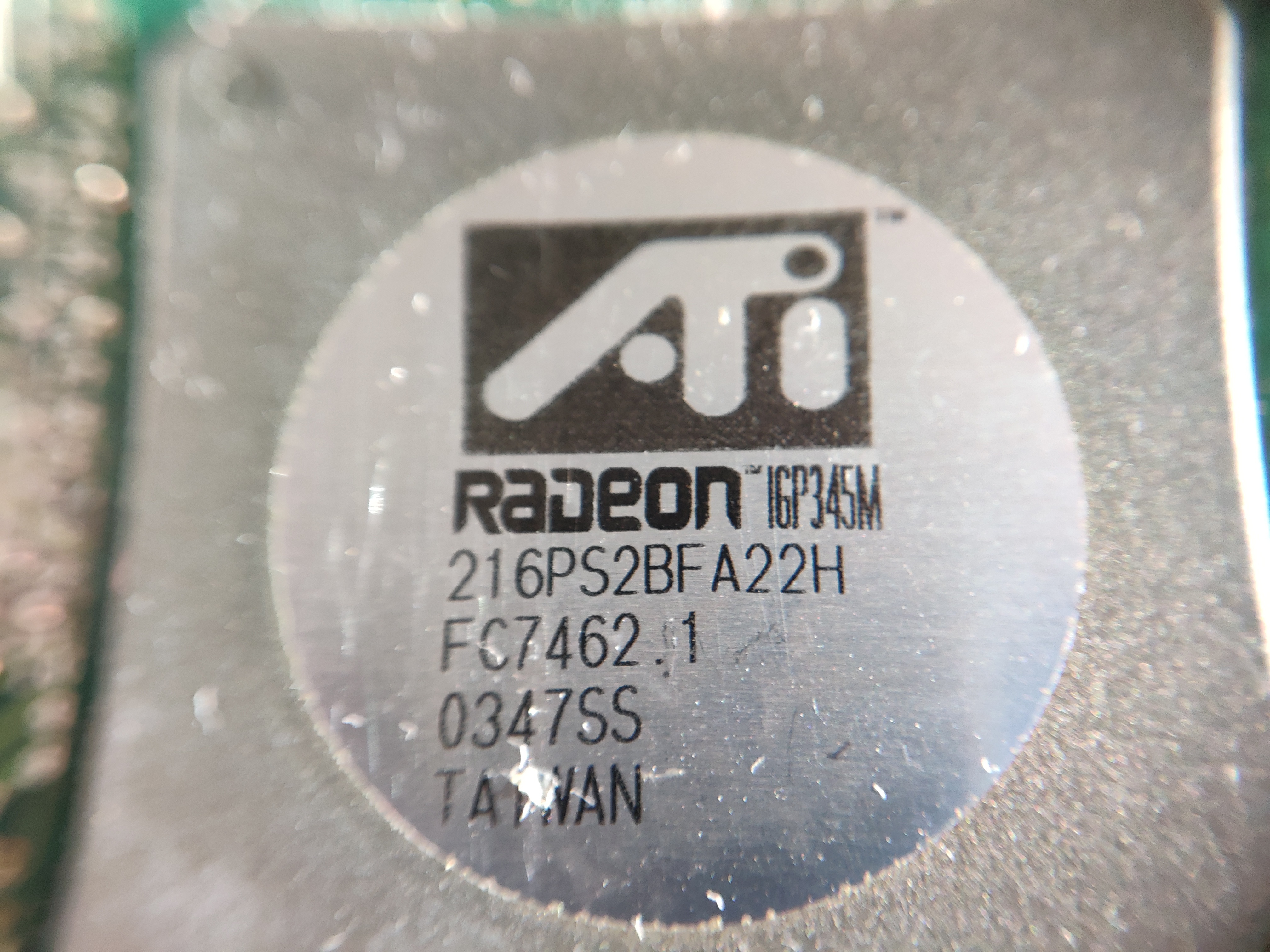
ATi Radeon IGP 345M - 2002 In the early to mid 2000s, it was the thing for graphics designers to get into chipsets. On the surface, it appears to make sense: GPUs already need high performance memory controllers and bus interfaces, the things chipsets do. Chipsets were starting to integrate video (to various degrees of success), so it made sense for the video people to get into chipsets. ATI had just bought ArtX and with it the GameCube video processor and also an Intel Pentium 4 bus license to go on top of the AMD EV6 license it already had. ATi of Canada made this, the RS200. It was available as RS200L (low end desktop, 400 MHz FSB only, 150 MHz IGP), RS200 (533 MHz FSB support, 183 MHz IGP) and the mobile equivalents, RS200M and RS200M+. This, as IGP 325M, is the RS200M+ which is better than the RS200M in... in fact, nobody seems to know. The video portion was based on the Radeon VE, ran at 183 MHz and featured a single pixel pipeline. Hardware TCL was not implemented but the three texture mapping units were. The memory controller ran DDR SDRAM at 200 or 266 MHz and therein lay the problem. The Pentium 4 was already quite bandwidth hungry, it aggressively prefetched, squandering bandwidth all over. It was also running an IGP which was also bandwidth hungry, but only from single channel DDR 266. Bandwidth hungry became bandwidth starved. RS200, in any of its incarnations, was not well recieved. It did fill an IGP-shaped gap in Intel's lineup, but only at the very low end. As we see it here, it was in a huge HP Pavilion ZE5600 laptop with a 2.6 GHz Celeron processor and the ALi M1535+ southbridge. Not Celeron-M. Celeron with 62.6 watt TDP. The cooler was enormous, and the laptop as part of a range of HP and Compaq laptops which used full sized desktop Pentium 4 and Celeron processors. The heatsink alone in this was huge, two exhaust centrifugal blowers and a 40 mm intake fan. It was a big honking desktop replacement, but the ZE5600 was the low end of it. The similar ZE5500 had an Intel chipset. |
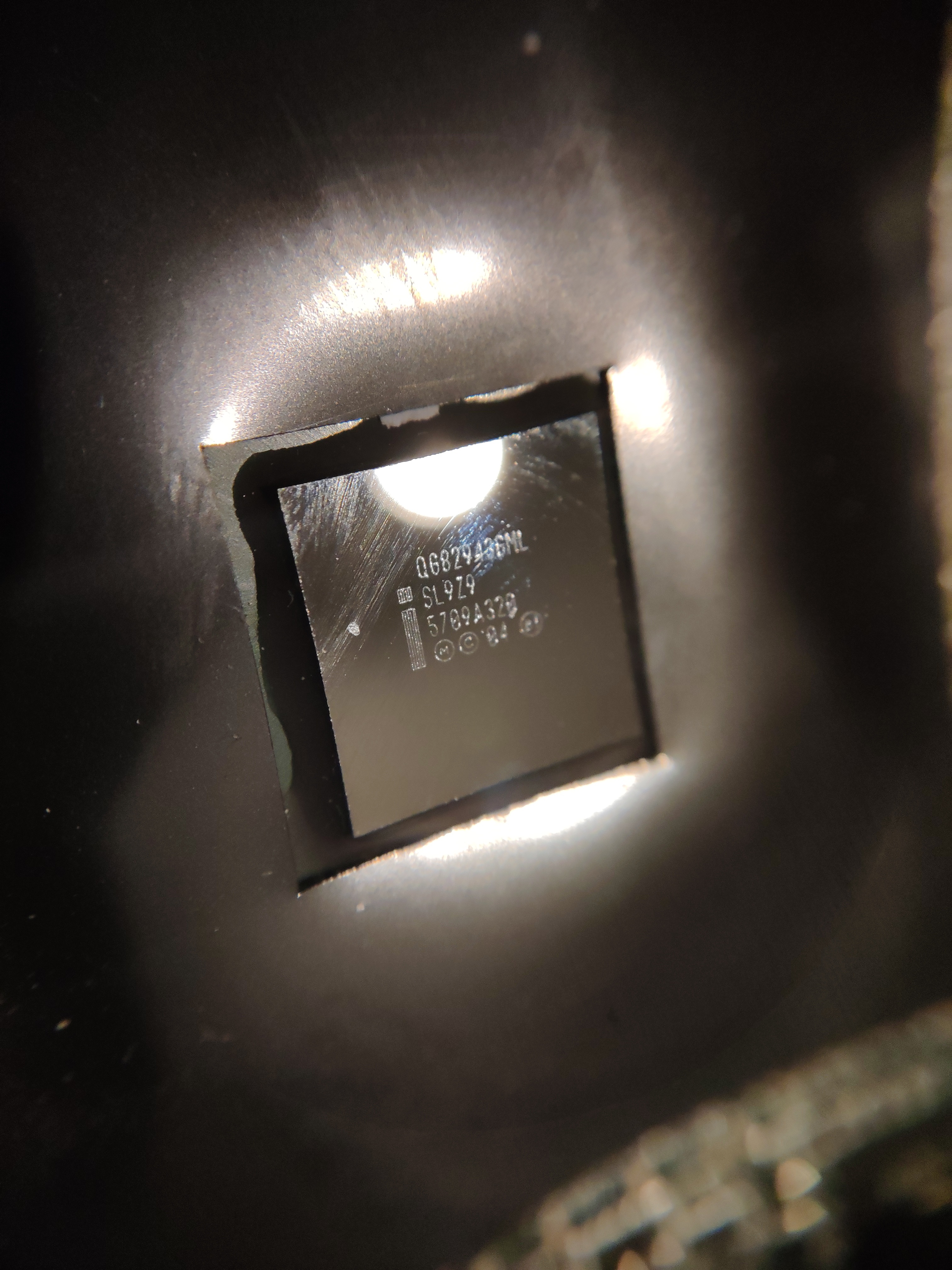 |
Intel Q943GLM Express "Calistoga" SL9Z9 - 2006 Intel's Core 2 platform on mobile was analogous to LGA775 on desktop. It used a 479 or a 478 pin socket (and both those were electrically almost identical, it was primarily to force incompatibility). This chipset, the QG82943GML tells us that it is the 943 model and the GML level. This means it is the Intel 943 Express chipset with graphics, mobile, and "low" or "light", so doesn't have all features enabled. In this era, Intel segmented on FSB and RAM speed restrictions. The two mobile sockets were "Socket-M" an "Socket-P", the former being 479 pin and the latter being 478 pin. This chipset supported "Socket-M" only, which was also known as mPGA479MN. Some sources will tell you Socket-P replaced Socket-M. These sources are paid by Intel. They ran concurrently for years. Socket-M was 2006, Socket-P was 2007, and you could still buy new laptops made with either socket in 2011. The 943GML chipset itself was released in 2008 with only Socket-M support and was the lowest end of the 945 Express variants other than an extremely bottom of the barrel 940 for Atoms. It wasn't entirely a die shrink of the earlier chipsets yet it was heavily derivative. It used what later became known as Gen 3.5 graphics, slightly improved from the previous Gen 3. Gen 3 in the 915 Express series was known as GMA 900, while Gen 3.5 was billed GMA 950. The difference was primarily clock rate. It had four pixel pipelines, two pixel shaders, vertex processing in software, and ran at a maximum of 400 MHz. In media decoding, it could offload MPEG-2 motion compensation, but nothing else, and sported a feature set of Direct X 9.0c. |
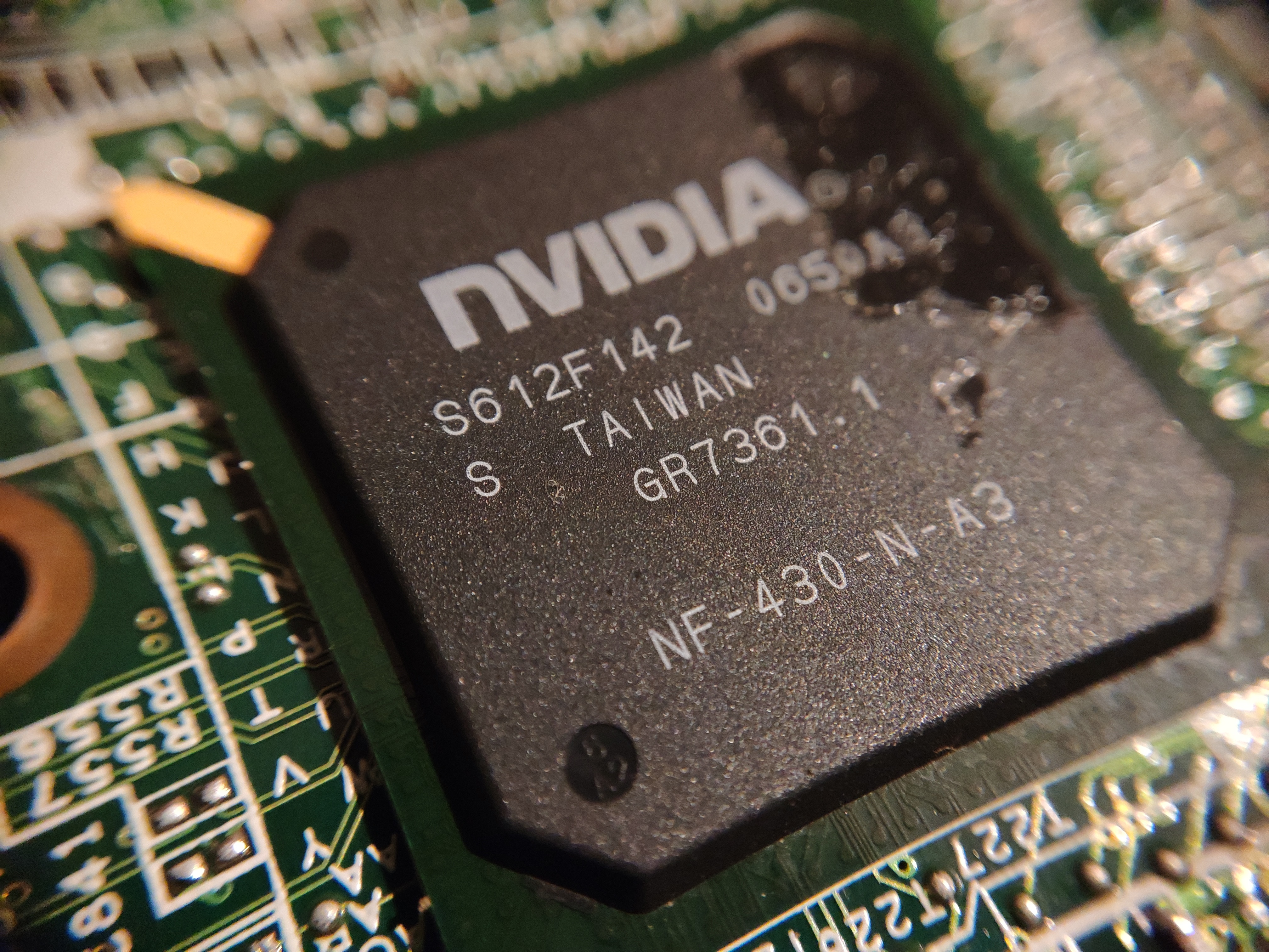 |
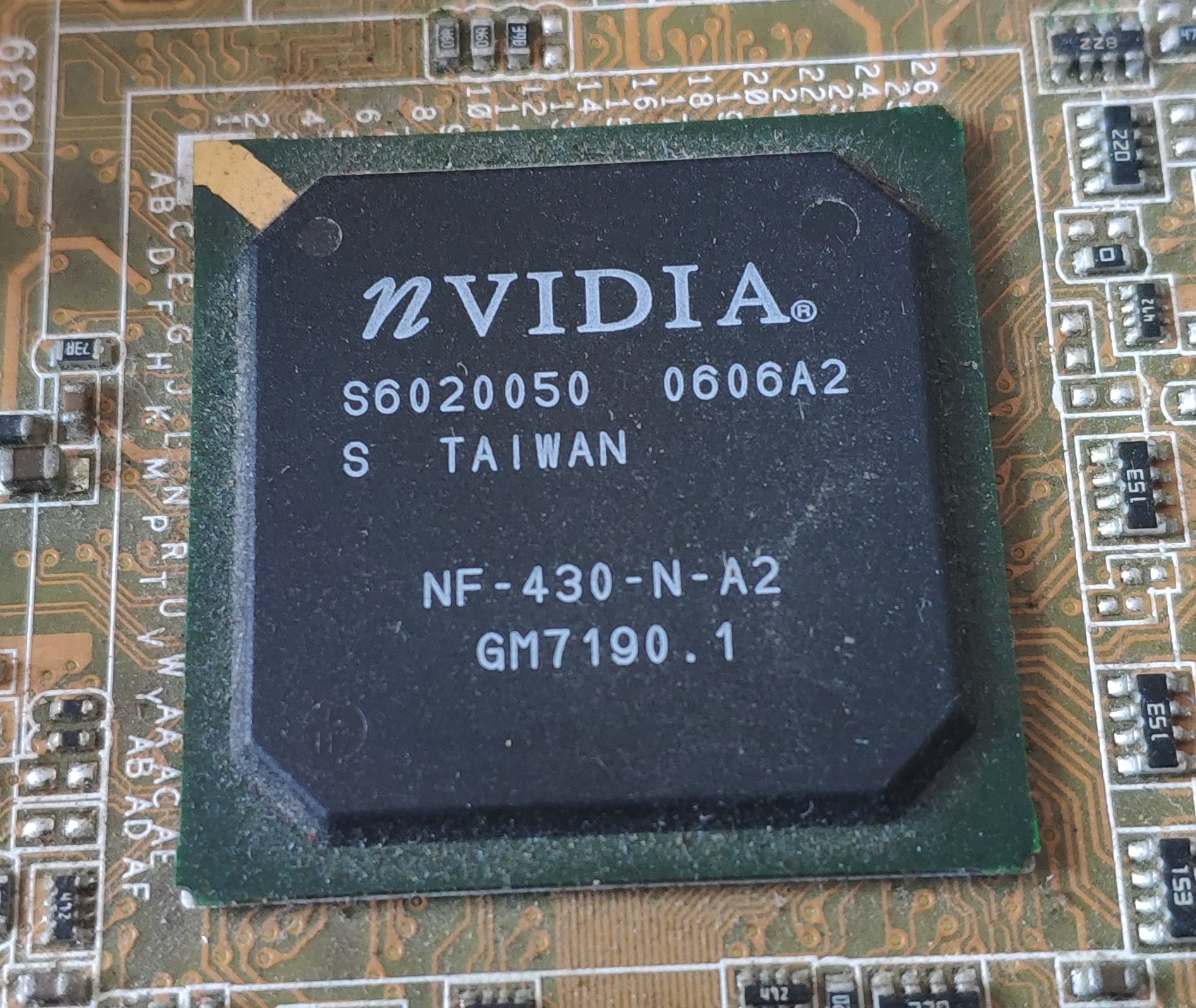
nVidia nForce 430 MCP61 - 2005 The popular nForce 2 was the best chipset on Socket A for a long time, and the first use of HyperTransport in the consumer space, where an 8 bit, 800 MHz HyperTransport link connected the northbridge and southbridge. nVidia followed it up with the short lived nForce 3 for AMD's K8 processors, but nForce 4 (later refreshed to "nForce 400") was where it was at. For the modern reader, this may seem unusual. Why's NVidia making AMD chipsets? AMD and Nvidia were very friendly in that day. They'd collaborated on the system architecture for XBox, before Microsoft decided to shift it to Intel, and the Nvidia "Crush" chipset was the result of that collaboration. Already co-developed and designed, it was easy to shift it over from the console to the desktop Athlon/AthlonXP platform. With the AMD K8 processor moving the memory controller to the CPU die, the nForce chipset didn't need to provide it, so the traditional northbridge and southbridge were merged into one product for the low end, the product you see here. It was, sadly, not very well regarded. The motherboards which used it were generally pretty good. This one in particular is a mobile version from a HP dx6000 series laptop. It failed due to the solder balls under the chipset cracking. This nForce 430 chipset in particular, on a HP laptop, was repaired once using a lot of aluminium foil shielding and a blowtorch to reflow the solder, but once it's happened it'll happen again. nForce 4 in this incarnation supported 20 PCIe 1.1 lanes, 10 USB 2.0 ports, 4 SATA ports, 2 PATA ports, 1 GHz HyperTransport, eight channel audio and onboard Gigabit Ethernet. A software firewall licensed by nVidia called "ActiveArmor" was available, this was universally regarded as unstable, terrible, non-functional and/or a complete waste of time. The onboard GPU, however, was not a complete waste of time. It was an NV40-based dual pipeline with one hardware vertex procesor, two pixel shaders (SM3.0) two TMUs and one render output pipeline. The pixel shaders ran at one operation per clock. This was, for an IGP, decidedly not awful. It wasn't good, nowhere near it, but it wasn't awful and this was an era where IGPs were awful. |
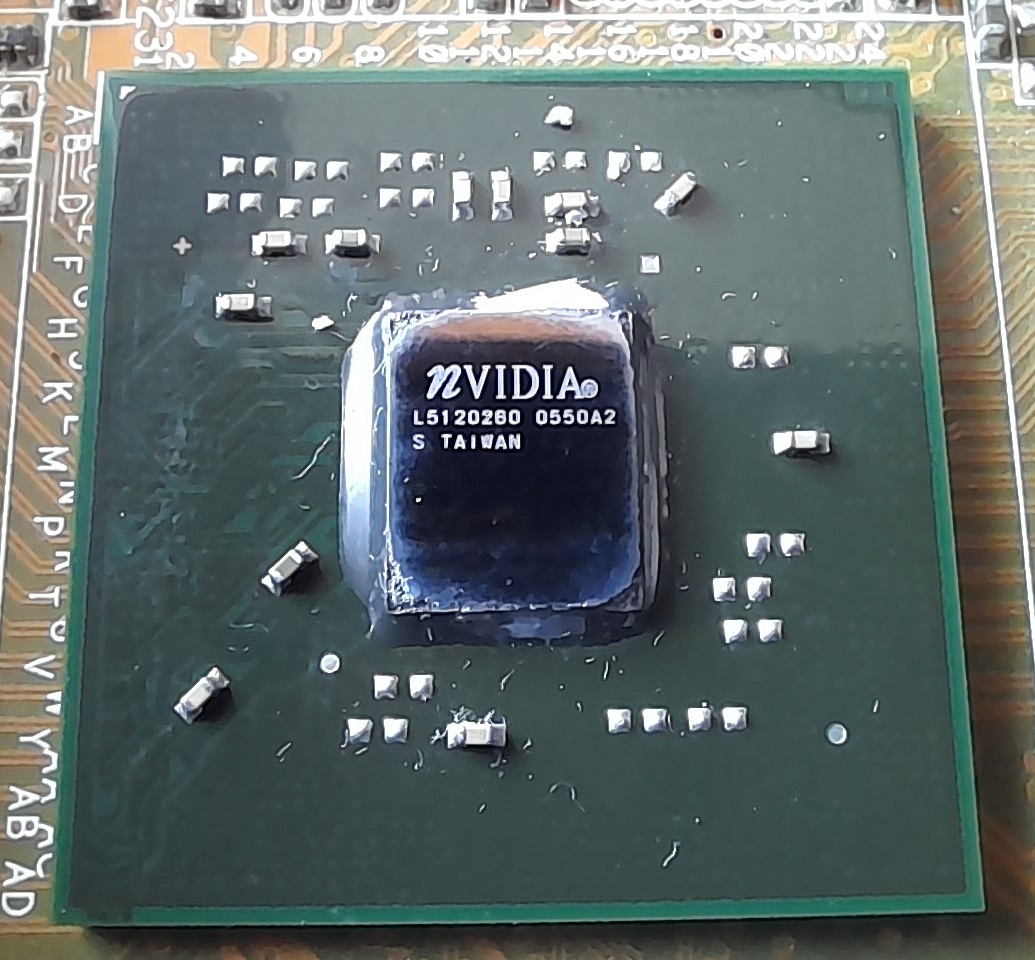  |
NVIDIA GeForce 6150 + NVIDIA nForce 430 MCP51 - 2005 This is the desktop version of the mobile parts both above and below. It uses the C51 core logic and the MCP51 southbridge, though the latter is branded NF-430-N. These late model nForce 4 series chipsets came after the rebranding done in 2006, the C51 northbridge has no branding on it at all and merely the L5120280 production code. MCP51 was the desktop higher power variant of the nForce 400 series, MCP61 was the low power and mobile, notably having far fewer PCIe lanes, a feature not as important in mobile. This one was used in an Asus A8N-VM CSM motherboard where it was paired with an Opteron 165 and four 512 MB DDR memory modules. It was retired mid-2010s as Windows 7 and 2 GB RAM became just insufficient. |
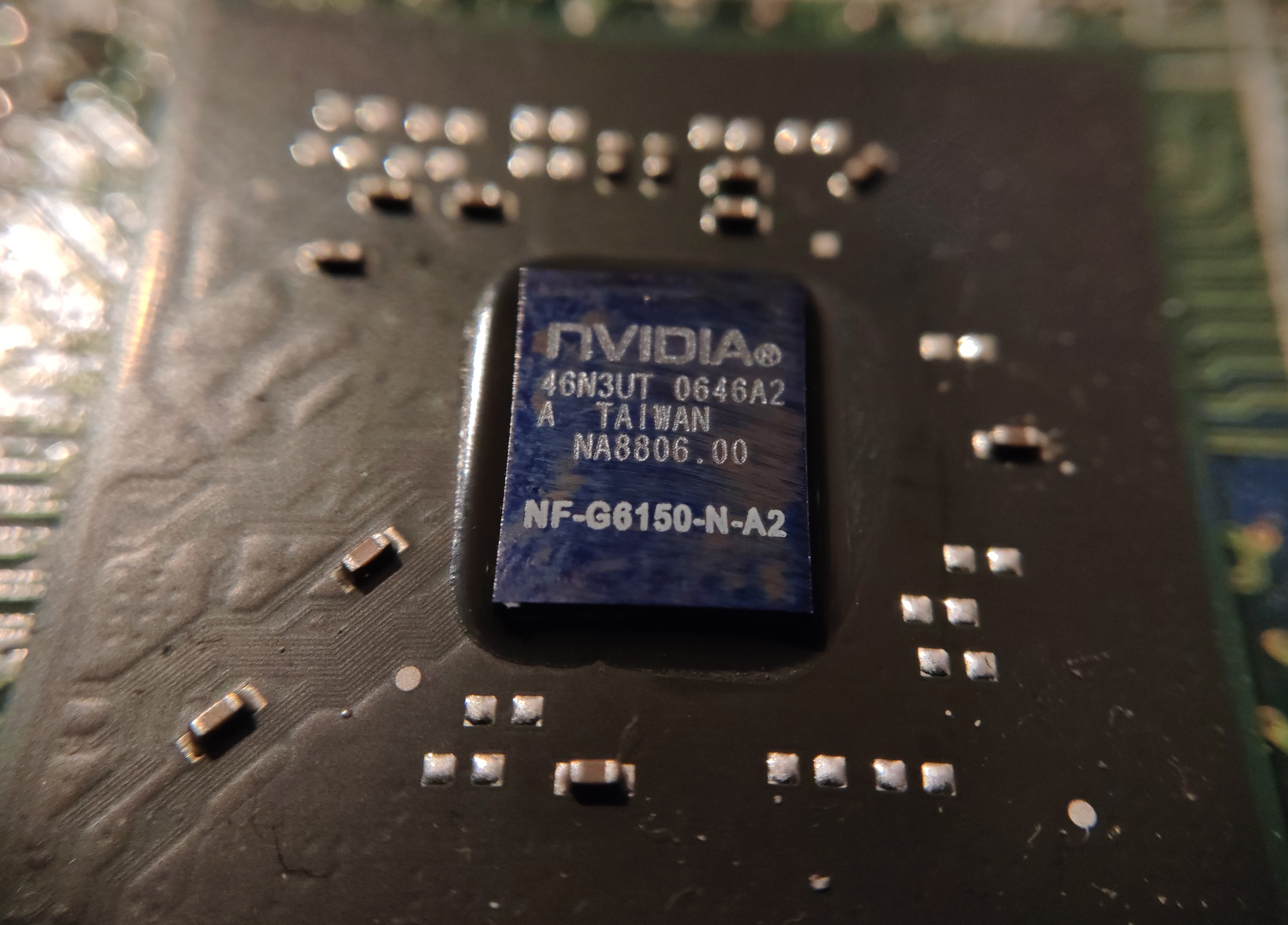 |
nVidia GeForce Go 6150 + nForce Go 430 MCP51 - 2005 This variant on nForce 4 was billed as "NVIDIA GeForce Go 6150 + nForce Go 430". Feature set is mostly identical to the MCP61 above, but it runs the GPU at 425 MHz instead of 475 MHz. This one was mounted next to an AMD Turion 64 X2 and would have been a very competent laptop in 2006. |
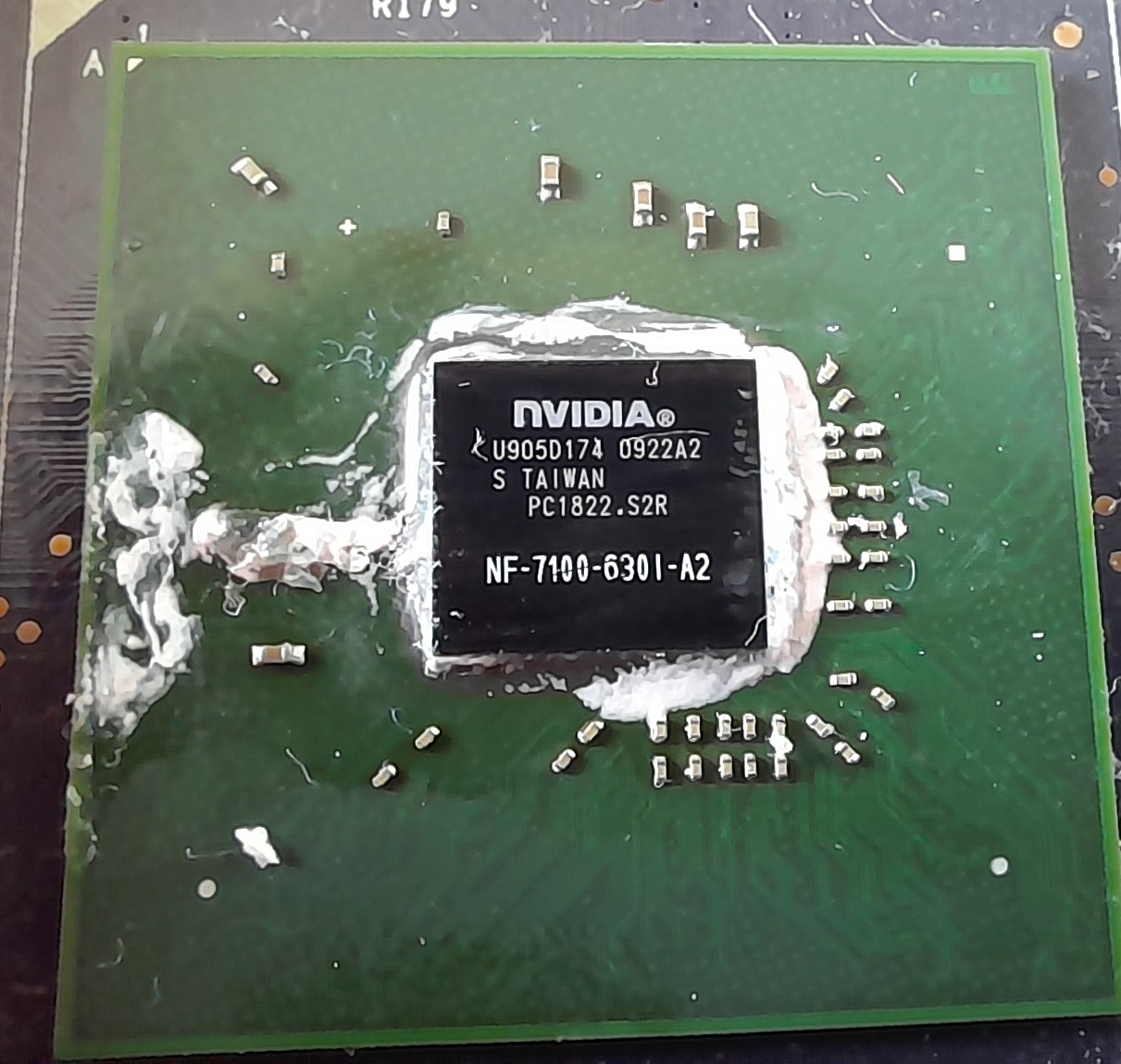 |
nVidia GeForce 7100 + nForce 630i MCP73 - 2007 The nForce 600 series on Intel was a weird thing. The ones with enabled IGPs had single channel memory only, when they're the ones which could benefit most from dual channel! They all could run a 1333 MHz FSB, but none supported DDR3, and all capped out at 800 MHz DDR2. MCP73 offered 18 lanes of PCIe 1.1, 10 USB2.0 ports, a single ATA channel, four SATA 3.0 Gbps ports, and gigabit ethernet. A fairly standard feature set, nothing special or spectacular, as MCP73 was aimed at the low end. This did not prevent it being abused, however, such as the system this came out of: A Packard Bell with a Core 2 Quad Q8300! The GPU, codenamed "C73", was doubled up from the nForce 4 series. It ran at 600 MHz and had four pixel shaders driving into two ROPs, but retained a single vertex shader. Nvidia didn't throw much more hardware at the GPU for three reasons: Chipsets are very low margin, so the 81 mm² die is about right, and that adding more GPU hardware would place more load on the already strained RAM bus. Finally, chipsets have a very limited power budget. |
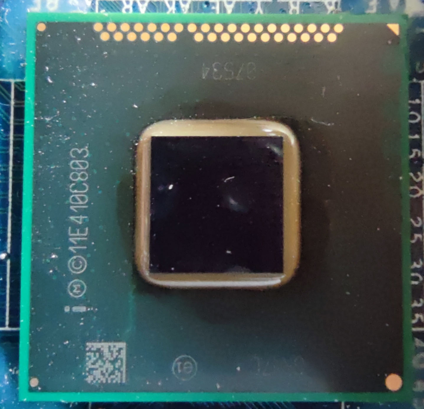 |
Intel QM-87 Lynx Point-M - 2013 Seen here as it lived in the wild, it represented a retooling of Intel platform controller hubs (PCHs) from 65 nm production to 32 nm production. Intel was not at all readily admitting that its PCHs were all just DMI2.0 devices and were technically compatible with any DMI2.0 CPU, Intel used slightly different sockets (literally, a few pins moved) and drew attention to new features like some more USB3 ports or an extra PCIe lane to show how the new platform was incompatible with the old. Or to hide the fact they were. Intel remained on the DMI2.0 platform from Sandy Bridge to Coffee Lake, with the low end H110 Skylake and H310 Coffee Lake platform only running DMI2.0. It broke out the DMI2.0 bus to 8 PCIe 2.0 lanes, four SATA 6 Gbps, 2 SATA 3 Gbps, 6 USB 3.0, 8 USB 2.0 and allowed the CPU to enable VT-d, which has nothing at all to do with the chipset! QM87 and its other "speed grades", HM86, HM87, and HM97, had a TDP of 2.7 watts and, seen here in a Dell Latitude E6440, didn't even have a heatsink. There was a C1 and a C2 stepping, but it's not clear which one this is as it has no relevant markings. |
|
Why did so many nForce chipsets fail in the 2000s and early 2010s?
This failure mode is worth explaining. The EU banned lead in solder as the Restriction of Hazardous Substances (RoHS) Directive, so the semiconductor packaging industry moved to a tin-silver solder but had not updated its processes to account for the different mechanical behaviour of this solder (refered to as "finishing material"). It has a longer wetting time and has a substantially higher stiffness. Compounding the matter was that BGA ball pitches moved from 0.65 mm to 0.4 mm relatively quickly. Proper research was done on the topic as laptops, motherboards, video cards, and non-PC electronics were failing at a much too high rate. Thermal expansion would be slightly asymmetric and so put very high forces on some of the solder balls on BGA packages until the balls cracked. With the solder being less able to bend and absorb the forces (plastic deformation), the forces grew larger until the solder cracked under shear stresses. This happened in the corners first, but the outer balls would also be damaged or stressed, such that a manufacturing defect (e.g. an oxide inclusion) would be exposed. It wasn't just nVidia affected, but nVidia was worst affected of all chipset vendors - Apple MacBook and iMac devices using nVidia GPUs were also affected. This, and other issues Apple has with its suppliers (Apple demands the absolute lowest prices, and will absolutely not work with an Apple-like market leading company able to charge a premium), meant Apple did not use nVidia again, ever. Very famously, the Xbox 360 was affected, this was the cause of the infamous "Red Ring of Death". At peak, the Xbox 360 had around a one in four failure rate! Pcbcart has a good article listing why these defects happen, now we know about them. There's also a PDF from SEM Lab on the different failure modes of BGA parts. |
|