
| Generations |
Pre-3D (-1995) Texture Mappers (1995-1999) Fixed T&L, Early Shaders (2000-2002) Shader Model 2.0/3.0 (2003-2007) Unified Shaders (2008+) Featureset determines where a card will go, not its year of introduction |
||||||||||||||||||||||||||||||||||||
|
Explaining GFLOPS
|
Here this resource is using theoretical peak scalar MADD instruction throughput. We consider a MADD to be two floating point operations. This gives us a convenient means to compare the shader unit throughout its evolution from a DX7 TCL processor to the modern stream processors. MADDs can be performed by the transformation (vertex) and the lighting (pixel) parts of a DX7 setup engine and by the vertex shaders and pixel shaders of a DX8+ GPU, meaning we can directly compare their raw crunching power. Combined with our display of memory bandwidth and pixel throughput, every metric needed to rate these cards against each other is present. |
||||||||||||||||||||||||||||||||||||
|
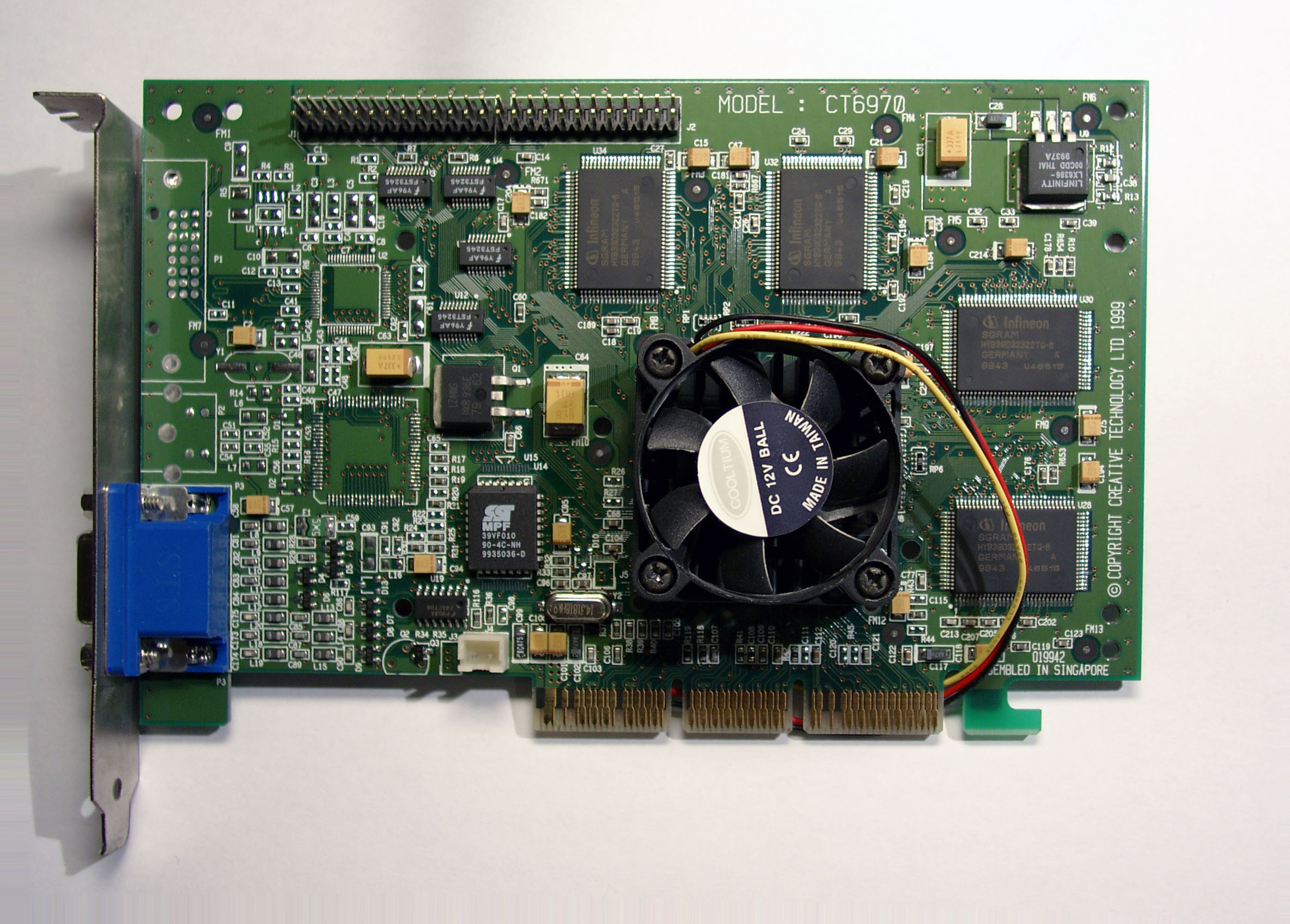
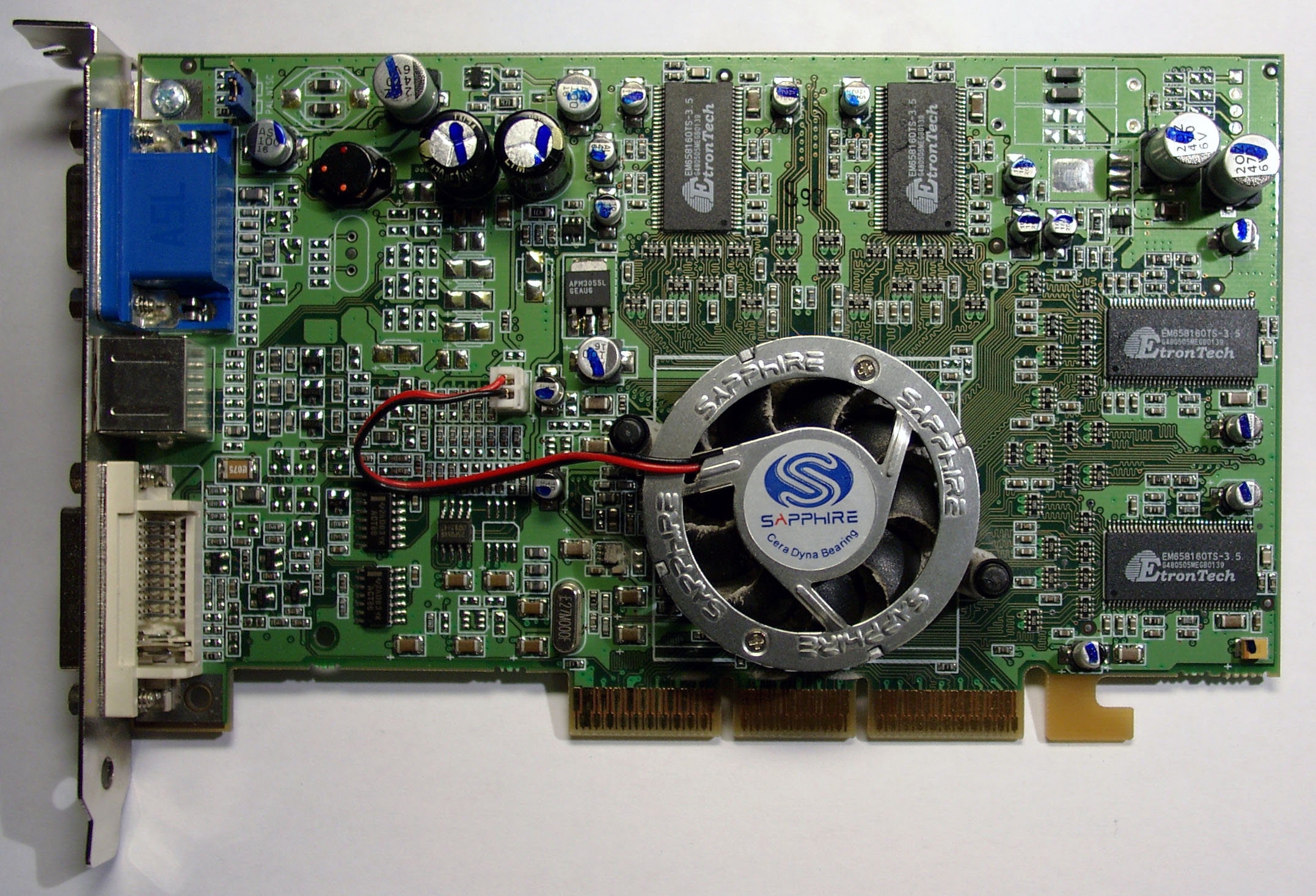
Creative Labs 32MB 3D Blaster Annihilator Pro (GeForce 256 DDR) - 1999 On release in late summer of 1999, the GeForce was impossibly priced, you could buy three Voodoo3 3000s for the same price, four if you shopped around. They still sold like hotcakes. Why? Because they were as much as twice as fast as anything else on the market. This card ran the NV10 GPU at Nvidia-approved 120 MHz and the RAM at Nvidia-approved 150 MHz. Even though it was choking for bandwidth and the RAM was actually rated for 166 MHz! GeForce overclocked very well, you'd usually get around 150-170 MHz from the GPU (this didn't matter) and maybe, if you were very lucky, 175 MHz from the RAM (this did matter), since 166 MHz DDR memory was the very, very cutting edge of what was possible. In mid-2000, all this would cost you $270 on the street and represented the highest specification video card of its day, the DDR versions of GeForce were very rare until much later in 2000. Correcting for inflation, this impossibly high end video card (NOTHING was faster) was $476 in 2023 US dollars. Creative was also a premium brand, which would have added a maybe $10-$30 to the list price. Geforce's performance wasn't from the hugely hyped transformation and lighting unit, but from the very fast DDR memory and the extremely wide four pipeline core in a world where two pipelines was good. While Geforce's core clock wasn't terriby high, it didn't need to be. The 4x1 Geforce could be clocked at 75 MHz and still have all the performance of a TNT2 Ultra, the previous king. While a lot of noise was made about the T&L unit, it was much ado about nothing. Games of this era were not nearly geometry heavy enough to tax the Geforce (Nvidia's "Village Mark" demo used upwards of 15x more polygons than Quake III, for example) and 3dfx among others noted that the types of calculations needed could be done very fast on a Pentium III (in SSE) or Athlon (in 3DNow!) anyway. DirectX 7 even came with a fast software T&L processor (known as "Software Vertex Processing") because the very same calculations had to be done in DirectX 5 and 6 anyway! One famous benchmark, which I believe may have been on Tom's Hardware, used a game which allowed selecting between Direct 3D's "Pure Hardware VP" and "Software VP". On a Pentium II 450, the hardware T&L resulted in better performance, but on a 600 MHz Athlon, the software VP was the faster! However, this T&L unit eventually gave rise to the vertex shader and pixel shader. The transformation part of it, which worked on vertex positions, could just as easily move vertices arbitrarily rather than rotate and skew them for proper perspective and position, while the lighting part, which computed the RGB lighting equations for each vertex, could just as easily work on other RGB data. These devices were widely parallel and each unit of the parallel array was called a shader. More flexibility to the shaders was added in Geforce 2, but it wasn't until Geforce 3 when a fully exposed programmable T&L unit arrived. Another first in the Geforce was full screen antialiasing. While 3dfx had the superior technology there, Voodoo5 had nowhere near the performance to adequately use it but for that matter, neither did Geforce. Geforce allowed 2x and 4x ordered grid supersampling, 2x would render 1.2x larger in each dimension to give twice as many pixels, then simply bilinear resize them down, 4x would render two times as large in each dimension to give four times as many pixels, then resize them down. The performance hit was astronomical but the quality improvement was welcome, especially in older games. Only a GPU with a proper vertex shader (or an accumulation buffer like Voodoo5) could do multisampling, so that didn't arrive until Geforce 3 either. This was a step change in game requirements. A CPU for gaming was one with a very powerful FPU, so AMD's K6 was not great, while Intel's P6 was. AMD's K7 was very FPU-endowed (actually more so than the decade-later Bulldozer!) for just this reason. This was because games did their geometry calculations on the CPU, which were all in floating point code. If the GPU could do this, CPUs wouldn't need so much FPU performance. Indeed, today, we don't even use the term "FPU" outside a very technical CPU architecture context, and then it usually means an FP execution unit. The GeForce inspired the revolution, but it was by no means part of it. By the time games needing hardware T&L arrived in quantity, GeForce was too slow and old to handle them. Also, I want to correct the record here. Some sites, notably TechPowerUp (and the hundreds of sites which copy its database) claim the GeForce 256 SDR had a 64 bit memory bus. Go ahead, click that link. Have a good look at the RAM on their example of an Asus V6600MX. Only half the RAM is actually fitted, so this one is 64 bits. Pretty clear it's using four 32 bit RAMs, and in two ranks, you can clearly see the traces going from one RAM to the next.. Then have a look at the Asus V6600 Deluxe SDR. Four RAMs again, but they're in QFP packages with a lot more pins. They're 32 bit RAMs and all of them go directly to the GPU: This is clearly a 128 bit bus. What was going on? There was a hidden SKU in GeForce 256 SDR, and Asus' name "V6600MX" hinted at it. While Nvidia didn't introduce the "MX" branding until GeForce2, it used it semi-openly with GeForce 256 for the 64 bit models. This was important! With only 1.1 GB/s of bandwidth, a 64 bit bus GeForce 256 SDR would underperform the previous generation. Nobody at the time seemed to cotton on to this trickery except AnandTech, and the 64 bit models were very common in the market when GeForce2 was released, but before GeForce2 MX - Seemingly Nvidia wanted to get rid of the remaining NV10 stock. Core: NV10 with 4 pipelines, 1 TMU each, 120MHz (480 million pixels per second) RAM: 128 bit DDR SDRAM, 300MHz, 4,800 MB/s Shader: None (DX7 transformation and lighting) MADD GFLOPS: ~2 Supplied by Ars AV forum member supernova imposter |
||||||||||||||||||||||||||||||||||||
|
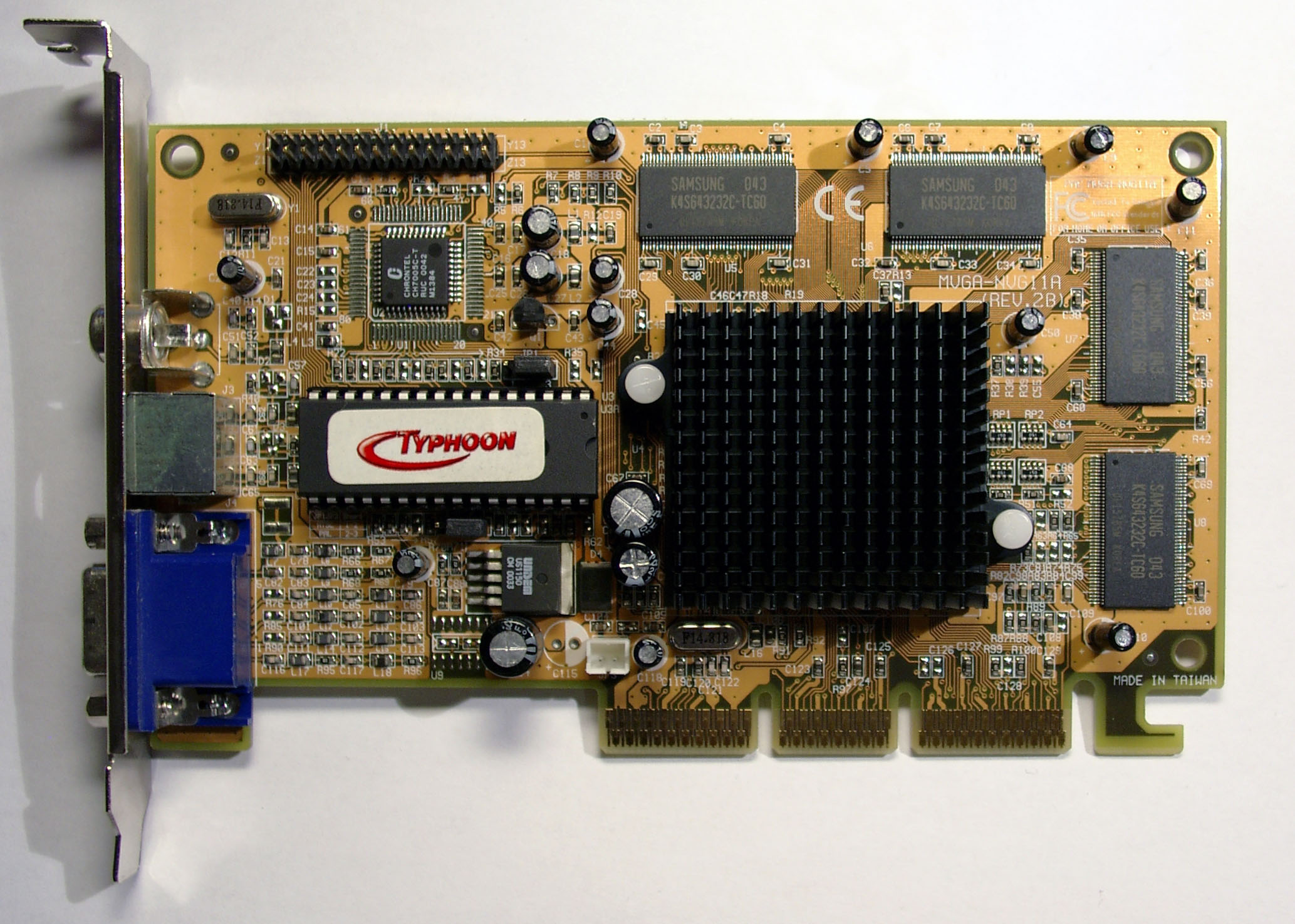
Anubis Typhoon Matrix II MX (Geforce 2 MX / 32MB) - 2000 The original Geforce 2 MX was scarily cost-effective. Offering almost all the performance of the previous-generation Geforce just one year later and for half the price it flew off the shelves. The only difference was that half the GPU was missing. This made it 2x2 and with 2 T&L units, so it had all the fillrate of the original Geforce since almost every game was multitexturing by this stage and the GF2MX had a significantly higher clock. In reality it was almost exactly between the DDR and SDRAM versions of the original Geforce and so for the price point, it rapidly ensured that no DX6 generation parts (such as Voodoo3, Savage4 or Rage 128s) would ever sell again, even though they were still widely available in 2000. Core: NV11 with 2 pipelines, 2 TMU each, 175MHz (350 million pixels per second, 700 million texels per second) RAM: 64 bit 333MHz DDR SDRAM, 300MHz, 2,666 MB/s Shader: None (DX7 transformation and lighting) MADD GFLOPS: 2.8 Supplied by Ars AV forum member supernova imposter |
||||||||||||||||||||||||||||||||||||
|
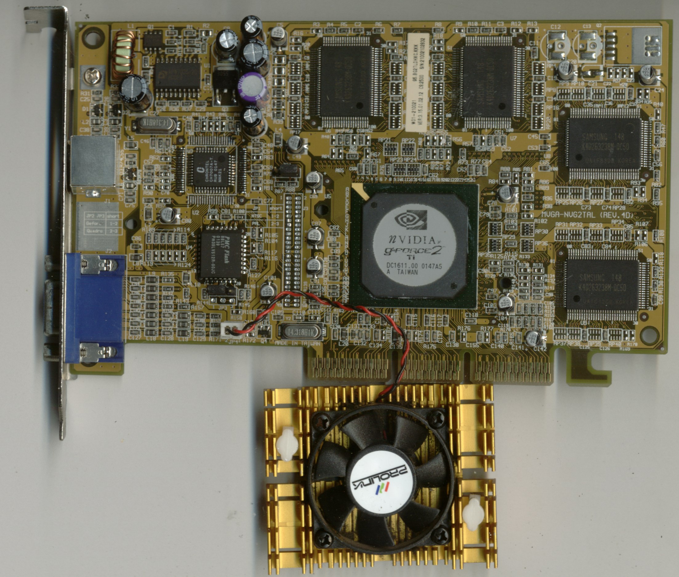
Prolink MVGA-NVG2TAL (Geforce 2 Ti / 64MB) - 2001 I'm not entirely sure whether this card is a Geforce 2 Ti or a Quadro 2 Pro. The card has a jumper on it to freely select between Geforce 2 or Quadro 2 - You can see the jumper just below the BIOS chip in the full size image (immediately above the fan power connector). The silkscreening between the two outputs tells us that both JP2 and JP3 (JP3 is not fitted) have to be at 1-2 for "Geforce" and 2-3 for "Quadro". JP3's "2-3" is a parking position, 1-2 grounds them. The switching is done entirely on JP2, towards the back of the card (with the ports) makes it a Geforce 2 Ti, towards the GPU makes it a Quadro 2 Pro. Since I believe all Quadros were branded and sold exclusively as "Nvidia" then a Prolink card probably isn't a 'legit' Quadro 2. Not that there was any difference. There should be little to no performance gained, the Quadro 2 Pro was clocked identically to the Geforce 2 Ti. With Geforce 3 being a little expensive and Geforce 2 Ultra being too expensive to continue producing when the GF3 cost so much already and beat the hell out of it, Nvidia launched yet another Geforce 2 in October 2001 - Geforce 3 lacked a "mass market" version like the Geforce 2 MX was, so Nvidia introduced the Geforce 2 Ti to be the mass market alternative to the Geforce 3 Ti 200 and Ti 500. Geforce 2 was discontinued entirely when NV17 was released as Geforce 4 MX. Nvidia could do this because they remasked the NV15 core for a 150nm process. The original NV15 was a 180nm part. This makes the GF2 Ti very overclockable, most would hit 280-300MHz, but as you will see the GPU wasn't the limit.
Geforce, as the original 256 and DDR, had started a paradigm which continues to this day, but they were very extreme cases. People started to notice that performance did not increase when the GPU clock was increased. The Geforce2 Ti was not faster than a Geforce2 Pro, even though the Ti had a substantial GPU clock advantage. However, the Ultra was noticably faster than either even though it had no additional computational resources over the Ti, all it had different was more RAM bandwidth. Contrast this with the TNT2, where overclocking the RAM had little impact but overclocking the core made all the difference. This was caused by 32 bit texturing. Gamers had slid over to wanting 32 bit rendering, but most developers still used 16 bit textures. Without the whole pipeline being in 16 bits, accumulation artefacts did not exist and the textures looked much better, even though they were the same textures. 3dfx's Voodoo3 rendered like this and did not exhibit "16 bit banding" even though its output was in fact 16 bit. By the time Geforce came around with four rendering pipelines, texturing was the limit of performance. Each pipeline wanted a 32 bit pixel value at the same time meaning that flat out, the 4x2 Geforce 2 running at 250MHz wanted: 8 x 250,000,000 = 2,000,000,000 pixel values per second (2 Mtexel fillrate) 2000000000 x 4 = 8,000,000,000 bytes per second That's not a mistake. Running flat out, a Geforce 2 at 250MHz wanted 8GB/s of memory bandwidth just for texturing. The Radeon HD 3450 further down the page barely has that! That's not all, though. The above calculation is for point sampled, point mipped texturing. We wanted trilinear filtered texturing. Trilinear filtering needs four samples each from two mipmaps and doing a trilinear texture sample in one cycle was the norm, meaning 8 samples in total, per TMU, per cycle. For trilinear filtered texture mapping, this Geforce 2 wanted 64GB/s. It's not quite that bad, not every opportunity to sample a texture is used, some effects go on in multiple cycles (such as fogging) but it does serve to show how incredibly bandwidth limited GPUs were even back then. Today it's even worse. We now have multiple technologies (e.g. texture caches on the GPU itself, fast Z-clear, multiple parallel memory controllers behind a crossbar, predictive memory access patterns, texture compression) to squeeze every last drop of data out of the memory and make every last bit count. The only reason the Geforce3 spanked the GF2 Ultra, when in fillrate it was behind the Ultra and bandwidth was equal to it, was because it had memory optimisations. Core: NV15Ti with 4 pipelines, 2 TMU, 250MHz (1000 million pixels per second, 2000 million texels per second) RAM: 128 bit DDR SDRAM, 400MHz, 6,400 MB/s Shader: None (DX7 transformation and lighting) MADD GFLOPS: 8.0 |
||||||||||||||||||||||||||||||||||||
|
Radeon 7500 64MB - 2001 By the time of the Radeon 7500's availability at the start of 2002 it was an entry level card to go under the Radeon 8500. Nvidia took a lot of flak for doing the same, pitching a DirextX7 level card at the same time as a DirectX8 card, but where Nvidia used the "Geforce 4" name for both, ATI did not. The Radeon 7500 was a derivation of the original R100 core in the very first Radeon. It had a few tweaks, notably dual-monitor support (One on VGA, one on DVI) and was a shrink to 150nm, previous GPUs had been 180nm. This made the RV200 core smaller, cheaper and able to run faster or cooler. As ATI were behind, they chose faster. It wasn't great and wasn't terribly good value for money as it came in at about Geforce 2 GTS performance. After a few months and the price came down, it became much more appealing. It was competing on the low end with the Geforce 2MX 400 (slower, cheaper) and on the higher end with the Geforce 2Ti (faster, about the same price) so it didn't sell well when new. The 7500 was the apex of the orginal three-TMU per pipeline R100 family and derivations of the RV200 core ended up in ATI's integrated Radeon IGP 320M, Radeon IGP 345M and Mobility Radeon 7000. This 2x3 design was quickly abandoned to favour the then-standard 4x2 and then to 8x1. Having more TMUs per pipeline offers increased texture fillrate (texels) but only when multi-texturing. Single textured surfaces use one of the TMUs in the pipeline and ignore the others, dragging down performance. As transistor densities rose, the savings of fewer pipelines became moot and the standard one TMU per pipeline arose, which would not be broken until ROPs (as pipelines became known after pixel shaders took over) were decoupled from TMUs. The RV200 must not be confused with the RV250 or RV280. The former is a version of the R100, the original 2x3 boneheaded Radeon. The latter two are versions of the R200, the Radeon 8500's GPU and used in the Radeon 9000 and 9200 series. Core: RV200 at 290 MHz with 2 pipelines, 3 TMUs per pipeline (580 million pixels per second, 1,740 million texels per second) RAM: 128 bit DDR SDRAM, 460MHz, 7,360MB/s Shader: None (DX7 transformation and lighting) MADD GFLOPS: 4.6 | ||||||||||||||||||||||||||||||||||||
|
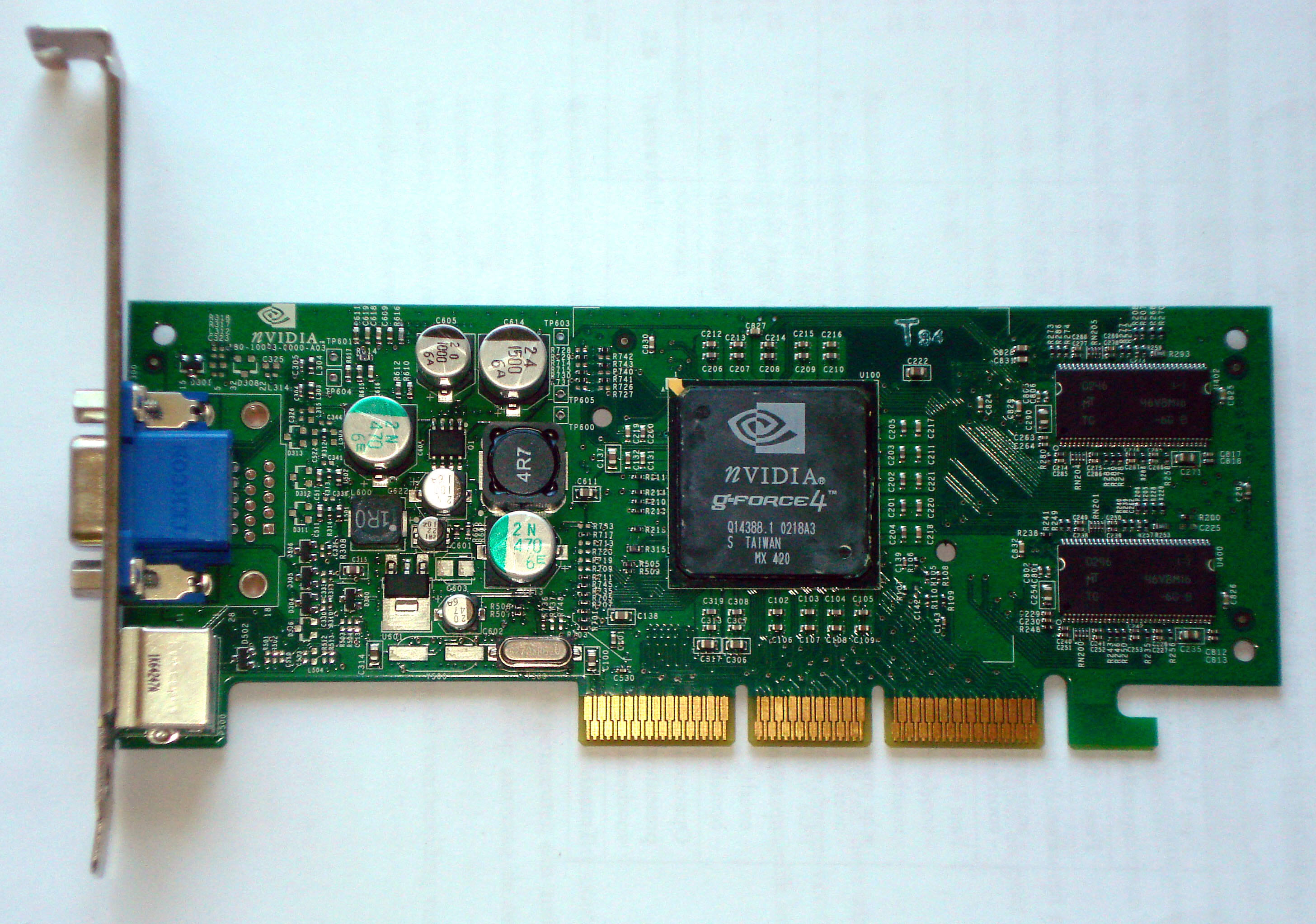
Geforce 4 MX 420 - 2001 The Geforce 4 MX series was one of the most controversial releases Nvidia had ever made. The NV17 GPU was an upgrade to the NV11, the Geforce 2 MX and shared much architectural similarity. It wasn't on the Geforce 3 level (with shader model 1.1) nor the Geforce 4 level (shader model 1.3), instead it was a legacy fixed-function design released after the Geforce 3. To make matters worse, the performance range of the Geforce 4 MX was quite large. The MX 420 was really bad, the MX 440 was passable and the MX 460 was verging on the high end of mainstream - The MX 460 could beat a Geforce 3 in DX7 level games which were largely bandwidth limited. The MX 420, seen here, had only 50MHz core clock over the GF 2 MX 400 and generally did not difference itself from its much older ancestor, yet in retail cost about 40% more. Most of them were supplied with 32MB onboard memory, but some had 64MB, not that the amount of memory really made any difference. This made it quite remarkable for its lack of performance. The Geforce 4 MX 440 was roughly the equal of a Geforce 2 Ultra while the MX 460 was about the peer of a Geforce 3 Ti 200, both comparing well against the mainstream of the previous generations. The MX 420 was far behind, it did not outperform the GF2 MX 400 it was replacing and to many observers was a pointless exercise since it was obviously more expensive to make than the NV11 based GF2 MX. Dell used them in their mid-range Pentium 4 boxes (which had no onboard video chipsets) along with the extremely weak TNT2 M64 part. However, the Geforce 4 MX series was not all failure. The MX 440 was extremely effective for its price point and, to John Carmack while developing Doom III, a potential disaster. He worried that Geforce 4 MX cards would become popular (they did) and so retard the adoption of shader hardware (they did) and so restrain the development of PC video (they did). Nvidia showed their cynical mastery of the market by quickly ceasing supply of the Geforce 3 series (which obliterated all Geforce 4 MXs except the 460, but the MX 460 was only very slightly cheaper than the 'real' Geforce 4 Ti 4200) and cutting OEM deals with the MX 420. The MX 460 sank without trace (and was rapidly discontinued): It was competing with the Ti 4200, the Radeon 8500 LE and was woefully underequipped for its price point. The MX 440 was quite successful (I bought one, the Leadtek Winfast A170DDR) while the MX 420 was mostly seen in crap that Dell vomited forth. Which is where this one came from. Funnily enough, the Geforce 4 MX series remained in production at least as long as mid-2007 as the Geforce PCX 4xxx series. Modelled on the MX 440 specs, they're able to out-perform a Geforce FX5200 across the board. They were a bottom-of-the-barrel solution for PCIe video. Core: NV17 with 2 pipelines, 2 TMU, 250MHz (500 million pixels per second, 1000 million texels per second) RAM: 128 bit SDRAM, 166MHz, 2666MB/s Shader: None (flexibility in the T&L unit was able to provide 'hardware assist' to vertex shader 1.1 in some beta drivers, but no pixel shader was possible) MADD GFLOPS: 8.0 Thanks to Kami for providing the part. |
||||||||||||||||||||||||||||||||||||
|
Leadtek Winfast A170 DDR - 2001 This is not the exact picture of the video card I had, but it is the exact same model. It replaced a Voodoo3 3000. The heatsink, as you can see, is mostly there for show, this card's actual power requirement was about 25-30 watts. In this era, the GPU was far more powerful than it needed to be but RAM hadn't kept up, so you could bump GPU core clock as high as you liked, but performance would increase only marginally. CPU bottlenecks weren't really a thing back then (they're overblown even today) and everyone was usually GPU bandwidth limited, though the less educated would call this a "fillrate limit". You could try overclocking the RAM, but you wouldn't usually get far, it was already being run as fast as it could handle. So, with 6.4 GB/s on tap, this MX 440 actually ran really quite well. As I recall, it was about �70 in 2002 and bought because the Voodoo3 really, really was long in the tooth and its 16 MB VRAM was extremely limiting. Mine ended up in a dual Pentium-III 450 (at 600 MHz) machine, which I left with a former girlfriend in Scotland, plugged into a Shuttle HOT-649A motherboard. The well-travelled machine came to me from the United States and eventually died in Scotland, it was left intact with her, but I don't doubt she binned it or something unbefitting of its stature. Core: NV17 with 2 pipelines, 2 TMU, 275MHz (550 million pixels per second, 1100 million texels per second) RAM: 128 bit DDR SDRAM, 200MHz, 6400MB/s Shader: None (flexibility in the T&L unit was able to provide 'hardware assist' to vertex shader 1.1, but no pixel shader was possible) MADD GFLOPS: 8.6 The latest drivers are ForceWare 93.81 Beta and 93.71 WHQL. |
||||||||||||||||||||||||||||||||||||
|
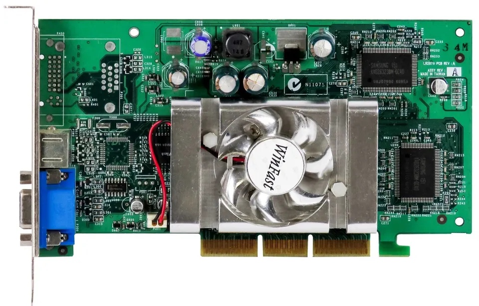
Leadtek Winfast A170 DDR T - 2002 Leadtek made many Winfast A170 DDR models. I had one at the time, somewhat larger than this with a curved aluminium heatsink. There were the A170 DDR, A170 DDR Pro, A170 DDR-II, A170 DDR T, A170 DDR Pro TH...All Leadtek's Geforce 4MX cards were "A170 DDR". No idea which one this is. It's an A170 DDR of the MX440 variety. It may be the MX440-SE, which was really more similar to the MX420, having only half the RAM bandwidth and a 64 bit bus. Mine was a 275 MHz GPU and 200 MHz (400MT/s) DDR memory, bog standard Geforce 4 MX440, but it was also on a larger PCB than this with active cooling. This one is somewhat newer, featuring BGA memory of unknown speed, two chips on each side of the PCB. Four chips, probably 32 bits per chip, giving the 128 bit width of an MX440 (a 64 bit width would be an MX420, but those usually used cheaper SDRAM). I believe - and this is only a belief - that the pictured card is the Leadtek WinFast A170 DDR T, which would be the GeForce MX 440-SE, and the specs will reflect this. As maligned as the Geforce 4 MX series was, the MX440 was very competitive for its price and did very well in DX7-class games. The lowly GF4 MX440 did better in Neverwinter Nights than a Radeon 9700, but NWN was enormously faster on Nvidia hardware. As a DX7 class game, it was also was highly bandwidth limited, so the 440-SE would not do very well. Most of them did not overclock well, the GPU was already bandwidth limited (it was at heart a Geforce 2MX) and the memory was the cheapest possible to fit the spec, so usually was running flat out anyway. This was, in 2002, the mid-range. Above it slotted the GeForce 4 Ti 4200, which was upper-mid, and below it was the GeForce 4 MX420, which was entry level. The DDR version of the MX420, this MX440-SE had the same memory performance: Twice as fast, but half as wide. In terms of absolute performance, in 3DMark 2000 it sat right next to the Voodoo3 3000 (from two years and three generations earlier!). It increased its stature as resolution went down, and its memory shortcomings were less well exposed. Core: NV18 with 2 pipelines, 2 TMU, 250MHz (500 million pixels per second, 1100 million texels per second) RAM: 64 bit DDR SDRAM, 200MHz, 3200MB/s Shader: None (flexibility in the T&L unit was able to provide 'hardware assist' to vertex shader 1.1, but no pixel shader was possible) MADD GFLOPS: 8.2 |
||||||||||||||||||||||||||||||||||||
|
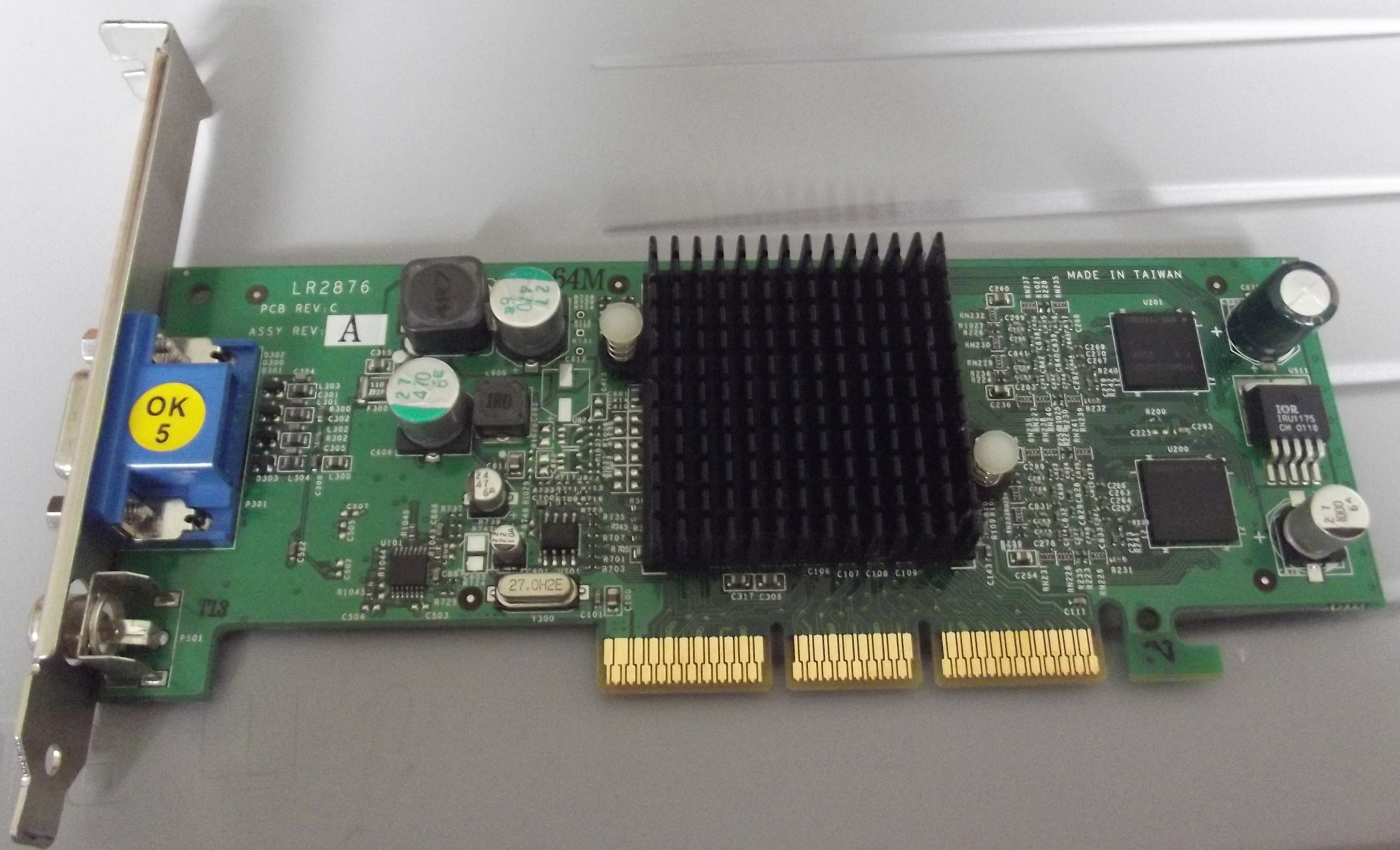
Geforce 4 MX 440-8X - 2002 A refresh of NV17 to NV18 added nothing but AGP-8X support (which GF4MX never needed to begin with) but importantly made it cheaper to produce, refined it a little for lower heat (and so a slightly higher clock) and better yield. They weren't seen very often as "Geforce 4MX", though, usually they were put behind a PCIe bridge chip and sold as the Geforce PCX 4000 or on AGP as the Geforce MX 4000. The MX440's 270MHz NV17 became the MX440-8X's 275MHz NV18 and performance was virtually identical between the two, as they were more or less the same part. The more interesting change to the 440-8X was the use of faster RAM. RAM usually has a very specific speed and density which is the best value and in the eight months or so between the MX 440 and the MX 440-8X, that had changed from the 400MHz DDR to the 500MHz DDR, the same 500MHz DDR which had been on the phenomenally expensive Geforce 3 Ti 500 and was on the Geforce 4Ti 4200. The increase of bandwidth had quite an effect, adding around 10% to the "-8X" version's performance. This particular one, labelled only as "NV18AT064C", doesn't even bear a visible Underwriters Labs number, so it can't be traced like that. The only sign that it even exists is on an outdated Jetway page, but Jetway resell all kinds of Taiwanese stuff with OEM packaging and no labels. This was the reference NV17/NV18 PCB design and the upper row of 8 RAM chips was optional. At launch, there were 64 MB and 128 MB variants, the 64 MB ones had only a 64 bit bus (the right side chips fitted, the top ones not) while the 128 MB models had the full 128 bit bus, and were much, much more powerful. Over time, denser RAM arrived and it became possible to put 128 MB on the 64 bit cards. As for its fate, check the capacitors on the upper right. Four are bulging, two are leaking. One of them, rated for 1,000uF measures at 210uF. After a replacement of these capacitors, it was put back into use. Core: NV18 with 2 pipelines, 2 TMU, 275MHz (550 million pixels per second, 1100 million texels per second) RAM: 128 bit DDR SDRAM, 250MHz, 8000MB/s Shader: None (flexibility in the T&L unit was able to provide 'hardware assist' to vertex shader 1.1, but no pixel shader was possible) MADD GFLOPS: 8.6 |
||||||||||||||||||||||||||||||||||||
|
Sapphire Atlantis Radeon 9000 Pro 64MB - 2002 The Radeon 9000 series was a rehash of the old R200 GPU (as opposed to the Radeon 9100, which was a relabeling of it!) and an abandonment of ATI's naming scheme of "7xxx = DX7, 8xxx = DX8, 9xxx = DX9". This was the RV250, which was R200 with the second level TMUs cut off and one vertex shader removed. RV250 would be further reduced into RV280 in the Radeon 9200 and 9250 series, meaning that the Radeon 9000 was faster than the 9250 and the 9100 was much faster than both! The Radeon 9000 Pro wasn't too bad but the price wasn't too good, decidedly mainstream pricing for an entry level part. The price would drop later (after the nerfing into the 9200), but almost two years later. Worthy of note is that the small cooler seen here on this Sapphire board was in every way identical to the one on the Radeon 9700! Core: RV250 with 4 pipelines, 1 TMU each, 275MHz (1,100 million pixels per second, 1,100 million texels per second) RAM: 128 bit DDR SDRAM, 275MHz, 8,800MB/s Shader: 4x PS1.4, 1x VS1.1 MADD GFLOPS: 12 | ||||||||||||||||||||||||||||||||||||
|
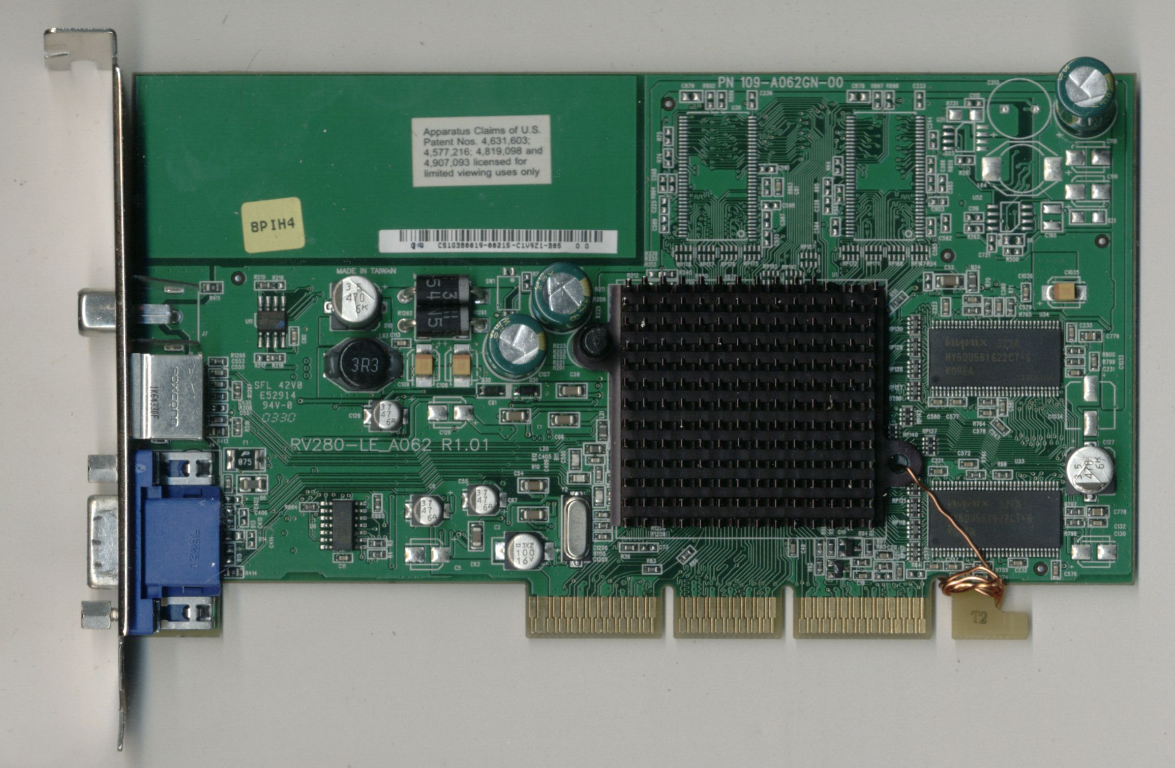
OEM Radeon 9200 LE 128 MB - 2003 As far as I'm aware the 9200 LE existed only from Asus. This card has a Hewlett Packard serial number on it, Asus being a HP supplier for a great many years. Identified as "RV280-LE_A062", this returns next to nothing on Google so yet again, this resource is going to fly to the top of the rankings. The RV280 is nothing more than the RV250 with AGP 8x support which on such a low end part meant absolutely nothing. The configuration is a simple 4x1 GPU with pixel shader 1.4 and vertex shader 1.1. RV250 was a die shrink of R200, the Radeon 8500 GPU, with the second stage TMUs removed. Compare it with the Radeon 9000 (released a year earlier) above. Basically, the Radeon 9200 series was identical to the Radeon 9000 series and the Radeon 9100 series was superior to both, as it used actual R200s from actual Radeon 8500 LE boards! The Radeon 9200 series was usually a 128 bit memory design, except the LE and SE variants which were 64 bit. To a word, they sucked. The R2xx series had always had very poor shader performance and RV280 did not break that mould. The 128 MB of memory onboard was no mistake, enough chips to match a 64 bit bus meant 128 MB was actually cheaper. Using less dense memory was actually more expensive! Cutting the chips was cutting the cost, hence half the spaces being missing. On the 128 bit boards, chips half as dense were used. The 9200 LE was a lot slower than the regular 9200 (same clocks, half the memory speed) and a little faster than the 9200 SE. They appear to have been made from surplus 9200 PCBs as, aside from the silkscreening, they are identical and ATI made no announcement of them. Core: RV280 with 4 ROPs, 1 TMU per ROP, 250MHz (1,000 million texels per second) RAM: 64 bit DDR SDRAM, 400MHz, 3,200MB/s Shader: 4x PS1.4, 1x VS1.1 MADD GFLOPS: 11 |
||||||||||||||||||||||||||||||||||||
|
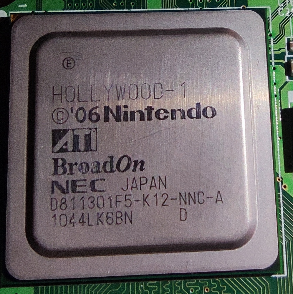
ATI Hollywood-1 As the "-1" variant, it is on a smaller substrate and has been shrunk to 65 nm from the original 90 nm. Hollywood is a minor technology update to Flipper, the GPU of the GameCube and, like Flipper, was designed by ArtX, a somewhat disgraced graphics IP company. ATi bought ArtX as GameCube was being designed. The "-1" variant merged "Vegas" and "Napa". "Napa" was the actual GPU and system bus controller, handling also RAM, audio, I/O, and 3MB eDRAM (2 MB framebuffer, Z-buffer, 1 MB texture cache). "Vegas" had 2x 24 MB MoSys 1T-SRAM as a L3 cache for the GPU only. Emulator authors have repeatedly said "Napa" is identical to GameCube's "Flipper" but for running at 243 MHz instead of 162 MHz. The second chip in Hollywood-1 (Vegas and Napa were merged in "-1") was a tiny third die containing a EEPROM and security lock out. Embedded in Hollywood is an ARM9 core (ARM926EJ-S) nicknamed "Starlet" which runs a secretive, undocumented, system management software referred to as "IOS" which runs what earlier systems would call interrupt service routines and I/O handlers. It also contains the hardware drivers for Napa. A game can load its own IOS from disc, but has to install it first. All software on the Wii specifies which version of IOS it wants. The Wii was not able to patch games or update IOS after the fact, and homebrew developers found that many earlier games performed massively better on later IOS revisions, but could never officially run them. As a GPU, Hollywood/Napa was extremely crude for the day. As an almost unchanged derivation of Flipper, it inherited Flipper's place in the world. It was designed to be cheap and more or less good enough in 1997. By 2006 it was patently inadequate, resulting in most Wii games being graphically basic. The Wii was not capable of HD output, and maxed out at EDTV (480p). ArtX gave Flipper and Hollywood a texture combiner, its "TEV", which was also used to generate image processing maps and results. Nintendo fans claimed the TEV was the GameCube's secret power, then later the Wii's, due to the massive long list of effects it could do. Most of them were hellishly slow and developers ignored them or used them sparingly. The TEV took four textures (which could be encoded texture-like data) and combined them, over sixteen clocks, in a primitive form of SIMD. The fixed-function T&L or TCL in DX7-class GPUs was similar to, but around a generation or two ahead of, the GameCube/Wii TEV. This is a confusing system. It was clearly designed with a hand-held option in mind, the very narrow and slow RAM, archaic GPU, and low power CPUs meant it absolutely sipped power. The Wii was tiny, most of its size taken up by the optical drive. Yet, Nintendo never made the handheld this system was so well suited for, instead relying on its ARM based Gameboy DS. Just off the image to the left is a single Hynix H5RS5223CFR GDDR3 SDRAM, standing in for the MoSys 1T-SRAM (masked-refresh DRAM) of the GameCube. Core: ArtX Flipper with 4 ROPs, 1 TMU per ROP, 243MHz (972 million texels per second) RAM: 32 bit GDDR3 SDRAM, 243MHz, 972MB/s Shader: None MADD GFLOPS: 9.4 |
 Hattix hardware images are licensed under a Creative Commons Attribution 2.0 UK: England & Wales License except where otherwise stated.