
| Generations |
Pre-3D (-1995) Texture Mappers (1995-1999) Fixed T&L, Early Shaders (2000-2002) Shader Model 2.0/3.0 (2003-2007) Unified Shaders (2008+) Featureset determines where a card will go, not its year of introduction |
||||||||||||||||||
|
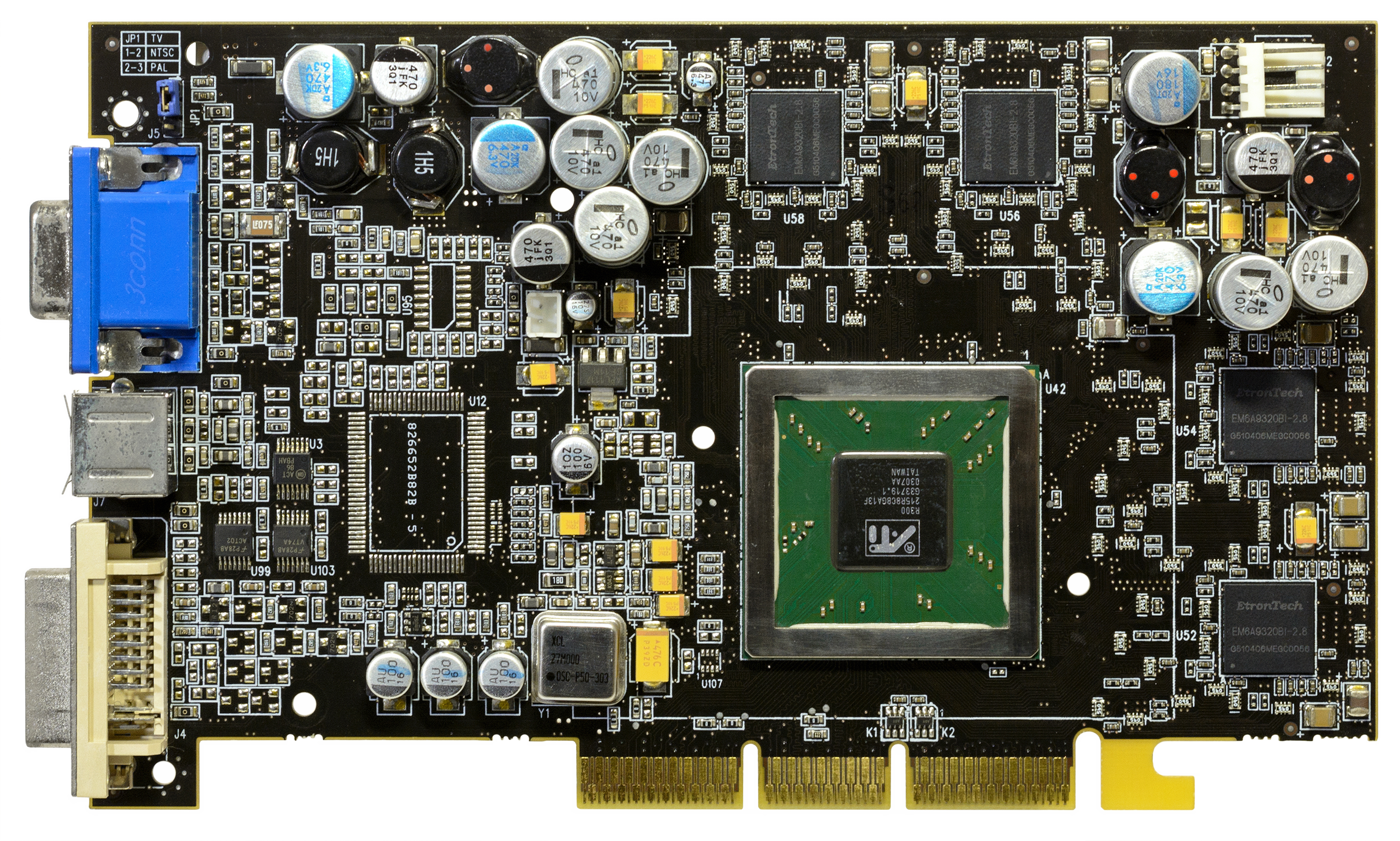
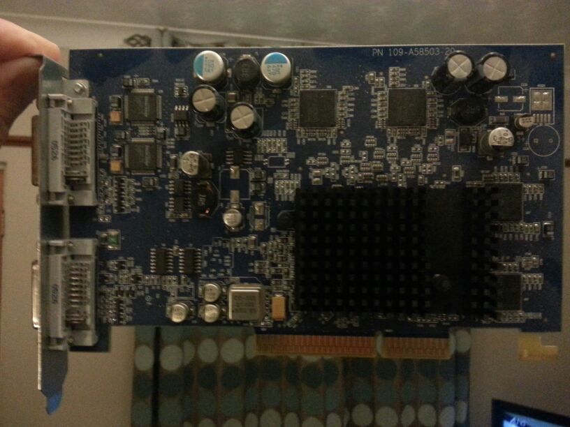
Sapphire Atlantis Radeon 9700 128MB - 2002 ATI had never really been able to compete in the big boy races, it'd always been either 3DFX or Nvidia who'd been at the top of things. Once 3DFX screwed themselves, it was just Nvidia although ATI tried, they really did, but dismal hardware, horrible drivers and senseless design decisions (R100's 2x3 architecture was moronic and R200 sacrificed a lot of render quality) always meant they'd be second best in a two horse race. Ther was another horse, however. ArtX was a company which was formed by ex-SGI engineers and hoped to get into the PC GPU business. A product was released, though it was somewhat poor and ended up in a forgotten ALI (Acer) Socket 7 chipset. ArtX then produced the underperforming "Flipper" GPU for Nintendo's underperforming "Gamecube" console, a 4x1 fixed function TCL chip which was R300's direct ancestor. ATI bought ArtX in 2000 and directed R300 development from there. In 1999 or so, ArtX had a very public spat with the website Ars Technica, where Ars proved that ArtX PR had lied, so ArtX invented fake witnesses and got them to post made up stories on the Ars website. The resulting PR backlash was a minor embarrassment. Voodoo2, Geforce (NV10), Geforce3 (NV20) are all names of products which stood beyond the competition with ease. It was with some surprise that 'Radeon 9700' was added to the list, the R300 GPU. The R300 was, put simply, a monster. It not only introduced Shader Model 2.0, it excelled at it. Normally being first to market is a poison chalice: The next product will have had time to refine the implementation, learn from the mistakes you made. So mighty was the R300 that a Radeon9700 (or Pro), released July 2002, was still competitive in mid-2006, four whole years later! Such a long lifespan was, quite frankly, absolutely unheard of in an industry with six-month product cycles and yet even by June 2007, a Radeon9700 would still out-perform some low-end solutions, such as the GeForce 7300 or Radeon X1300. To be still comparable with in-production cards after five years just shows how ridiculously powerful the 9700 was when it was new. By 2011, AMD's entry level was the Radeon HD 5450, which performed pretty much the same as the Radoen 9700 in games I had available to test. The 5450 had a much faster CPU (a 2.6 GHz Athlon X2) than the R9700 did (2.2 GHz Athlon XP) and performed similarly in Aquamark3 and Oblivion.
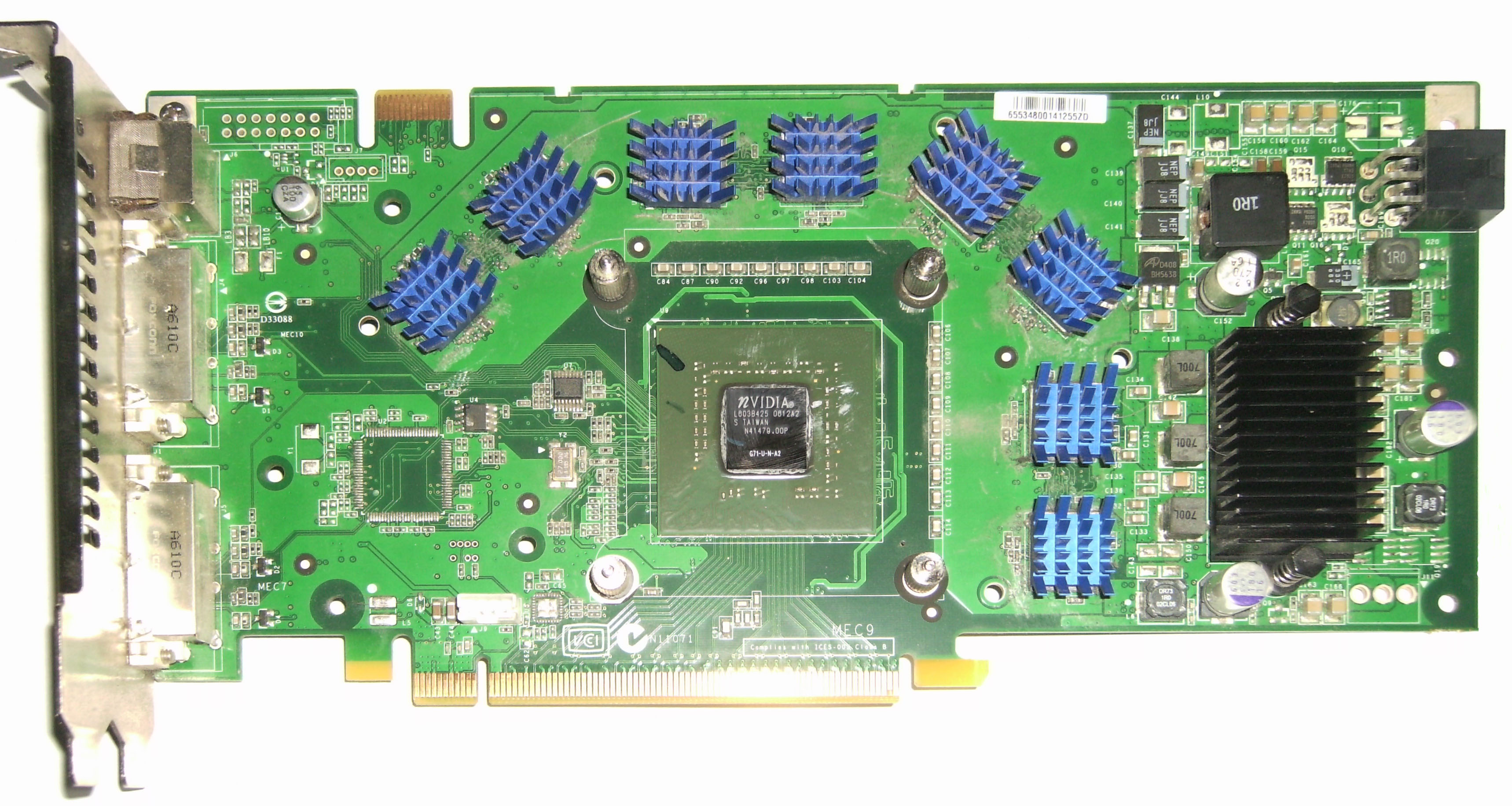
Most of the R300's massive performance came from its 256 bit wide memory bus, enabling almost 20GB/sec of raw memory bandwidth. This, together with its angle-dependent anisotropic filtering (AF), meant that using AF on an R300 carried little to no performance penalty in an era when performance hits of up to 70% were the norm for enabling AF. Most other video cards had four render output pipelines (ROPs) with two texture mappers each (4x2 configuration) so only reached their peak performance when multitexturing was in use. R300 carried eight (!) ROPs with one texture mapper each (8x1), so was running at peak performance all the time. The GPU wasn't all that different from ArtX/Nintendo "Flipper", the ROPs were very similar and the pixel shader obviously an extension of the fixed-function TCL in "Flipper". It appears, however, that ArtX owned the rights to the design and so needed to pay no royalties to Nintendo. ATI were rumoured to be having yield problems from the sheer size of the R300 GPU, 110 million transistors compared to the 61 million of the NV25 (GF4Ti) and wanting a "300MHz+" clock, when NV25 only barely scraped 300MHz. However, overclockers need not have worried. Most R300s were stable, depending on cooling, to 350MHz and even beyond. This particular card ran perfectly happy at 356MHz GPU clock (on stock cooling!) and 300MHz RAM clock, the RAM used in both the Pro and vanilla was not good for overclocking. At 356MHz the R300 was (to use a technical term) taking the piss. The specs for this particular card are a 270MHz GPU clock, a 277MHz RAM clock, 128MB of DDR-SDRAM (The R300 supported GDDR2, but never used it) and the usual VGA/DVI/TV connectors. The 9700 Pro was about 15% more expensive and featured a 325MHz GPU clock and a 310MHz RAM clock so for the performance was actually better value than the plain 9700. It also turns out the PCB I have is a later version, most were sold with a slighly different PCB. Just left of the GPU ASIC, most cards had an unfilled double pin header. Mine has an unfitted IC, labelled "U12". It is not clear what function this IC would have, and I can find no examples of similar cards with it fitted. So successful was R300 that R4xx and R5xx are all based on it and the Xenos GPU in the Xbox360 is, at heart, descended from the R300 (the ROPs are identical). A moment of respect for a former king, please. As an interesting sidenote, the Radeon 9500 Pro was meant to be the same 8 pipeline GPU with 128 bit memory, but DDR memory running fast enough (540 MT/s) wasn't widely available and, where it was, it was as 32 bit wide, 3.3 ns or 2.8 ns from Samsung (Hynix showed up later) with a 32 Mbit in four banks capacity, so 16 MB: Samsung K4D26323RA-6C2A was used here. This caused ATI a problem. How do you make 128 MB on a 128 bit bus when all you have are 16 MB RAM chips which are 32 bits wide? Use 8 of them, you now have your 128 MB... But your bus is 256 bits wide. Use 4 of them, your bus is 128 bits, but now you only have 64 MB. It seems ATI was relying on 2M x 32 (4 bank) memory arriving, but that didn't for some time after launch. So ATI just gave the 9500 Pro 256 bit memory initially and somehow reduced performance in software, probably by disabling bank access modes. This was fixable in software! Initially a hardware mod was needed but before long enthusiasts had worked out how to run the memory at full performance and, then, the 9500 Pro was just a 9700. The shenanigans didn't stop there. The 9500 "non-Pro" ALSO sometimes had 256 bit memory, but it had half the GPU's pipelines disabled... In software! Soft-modding these to the full 8 pipelines was also possible. Even those with 128 bit RAM (the 64 MB versions were always 128 bit) could still have the remaining 4 pipelines enabled. Later in their life the required 32 MB DDR RAM chips appeared and the PCB was physically 128 bit on all 9500-series cards. Drivers: Drivers included with WindowsXP (Service Pack 2), Linux (as r300). Core: R300 with 8 ROPs, 1 TMU per ROP, 275MHz (2200 million texels per second) RAM: 256 bit DDR SDRAM, 540 MT/s, 17280MB/s Shader: 8x PS2.0, 4x VS2.0, MADD GFLOPS: 29 I accidentally lost the high-res image for this, so have borrowed one of the same card from vccollection.ru. It is for illustration only and has no claim of title. |
||||||||||||||||||
|
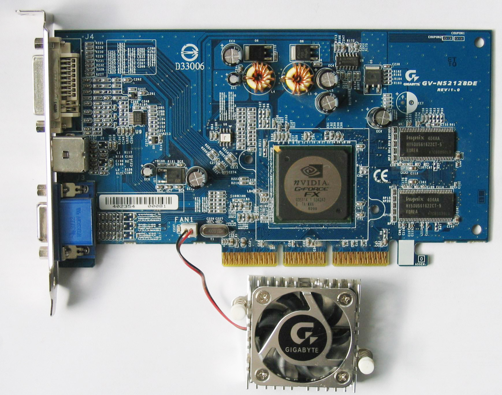
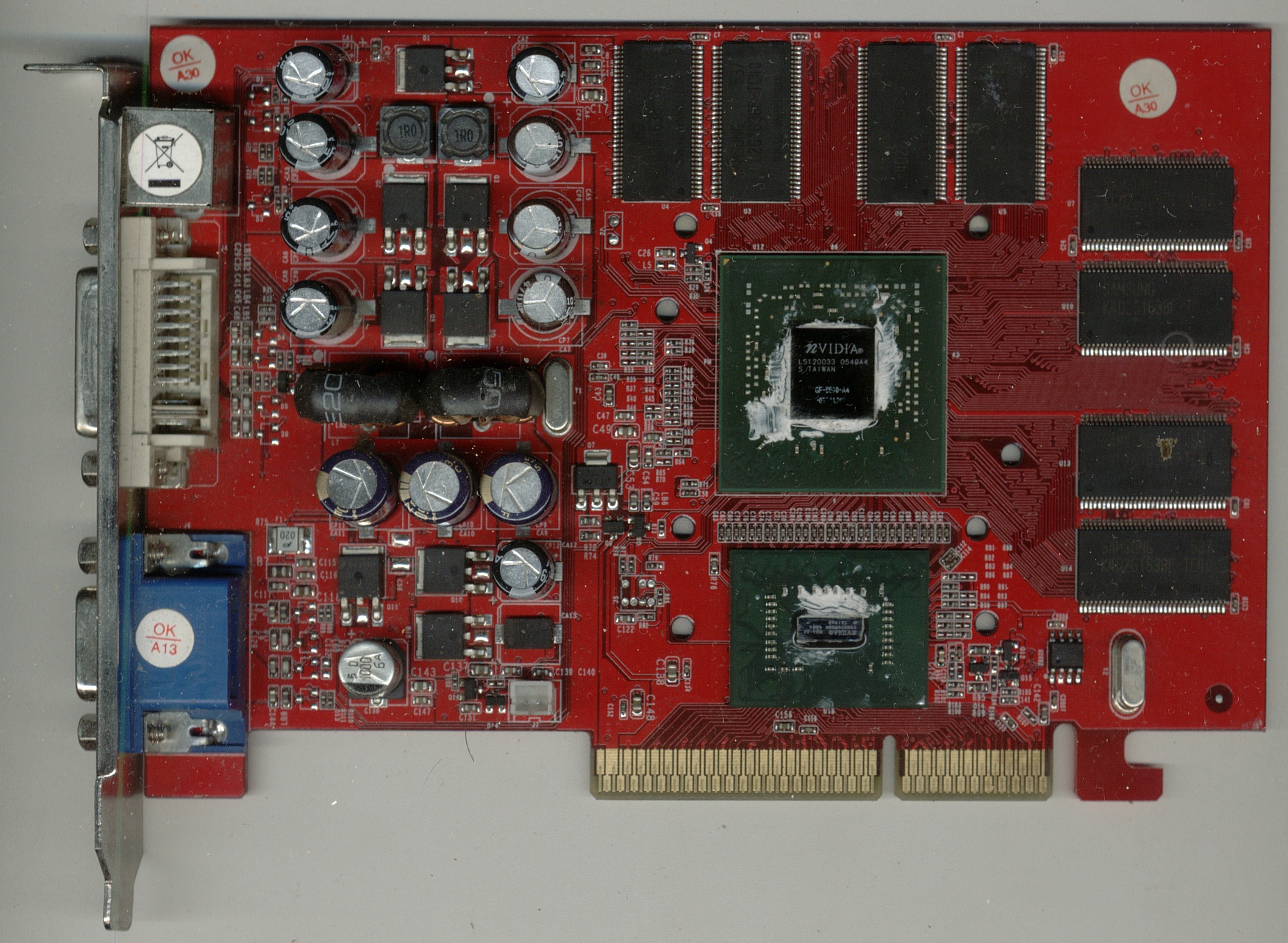
Gigabyte GV-N52128DE Geforce FX5200 128MB - 2002 This was about as slow as AGP video cards got and was a fairly standard FX 5200. Now the Geforce FX series weren't terribly great to begin with so one can imagine how bad the FX5200 was (about a tenth of the speed of a Radeon 9700, which was released about the same time). To be fair, it was very cheap and did beat integrated video...though not by much. It does still implement a full DirectX 9.0 featureset, so is compatible with Windows Vista's Aero Glass interface and will run Windows 7, though with the drivers in a compatibility mode. In a pure marketing move, most FX5200s were given 128MB of memory when both the memory and the GPU were extremely slow, warranting no more than 32 or 64MB. The memory on this card is bog standard (and incredibly cheap) 200MHz DDR, normally destined to go on PC3200 memory modules. An FX5200 loaded with the entire 128MB in use would be a slideshow measured in seconds per frame. I'll let the specs speak for themselves. Core: NV34 with 2 pipeline, 2 TMU, 200MHz (800 million texels per second)* RAM: 64 bit DDR SDRAM, 400MHz, 3200MB/s Shader: 1x PS2.0, 1x VS2.0 MADD GFLOPS: 5.5 The NV3x rasterisation pipeline was very weird. It could work on, in this case, four different pixels at once so long as they weren't being textured or part of a Z operation at the time. So the pipeline looks like "2 pipes, 2 TMU" or "4 pipes, 0 TMU" depending on how one looks at it. This meant the FX series could reach maximum fillrate quite easily and was technology NVidia aquired from 3DFX, to have been part of Spectre: NV3x could do stencil and colour operations "for free". Thanks to Filoni for providing the part |
||||||||||||||||||
|
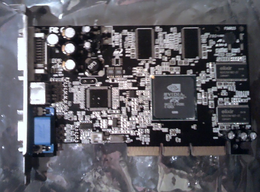
Inno3D Geforce FX 5200 128MB - 2002 They don't really get much worse than this. Let's start with the memory, 128 MB of Elixir N2DS25616B-5T. These are 256 Mbit capacity, 16 bit wide DDR SDRAMs. They'd commonly be found on PC3200 or PC2700 DIMMs, since they (the "5T" model) were rated for CL 2.5 at 166 MHz and CL 3 at 200 MHz. The Gigabyte card above uses a different vendor, but the specs are identical. DIMMs are 64 bits wide, so four of these would be needed for a 128 MB memory module, as cheap as it got back with DDR. Oddly enough, while the dominant FX 5200 was the 128 bit model, both samples here are 64 bits wide. With 128 MB it too uses four RAM chips. The PCB, as you can see, has provision for two more (and two more on the rear), but these would be 128 Mbit DRAMs and would give the FX 5200 a 128 bit bus and 128 MB. The GPU is an NV34, seen in every FX 5200 and the hilarious FX 5100. In this 64 bit model (even the FX 5200 was standard with 128 bit memory) the GPU is clocked to only 250 MHz. With a 2x2 pipeline and 166 MHz memory, it had just 2.7 GB/s of memory bandwidth, less than the TNT2 Ultra had several years before. It was cheap, slow and... well, just cheap and slow. Update: This actually went into use, providing video for a 3.0 GHz Pentium4-HT. In Aquamark3, it scored 7,300 (only 790 for graphics!), but then was overclocked to 298 MHz GPU and 432 MHz memory (without even trying, as it was still running passive). This improved its AM3 score immensely, to GPU 1,000 and total score 9,100, as the memory was overclocked by 130% of its standard value and all FX5200s, except the Ultra, were enormously memory limited. As shown, the card would not overclock any more than 298 MHz on the GPU. Even 300 MHz was just not quite there. Some of the detail above was also modified, as it turns out the standard 64 bit RAM FX5200 runs DDR400 memory, but this clocks to only DDR333. The standard GPU is also 240 MHz, this one runs 250 MHz. It does, however, use memory capable of DDR400... and, via overclocking, even higher. I'm told that with a few minor hardware mods (e.g. adding a fan!), the NV34 GPU was quite happy going to 400 - 500 MHz. Core: NV34 with 2 pipeline, 2 TMU, 250MHz (1,000 million texels per second) RAM: 64 bit DDR SDRAM, 166MHz, 2700MB/s Shader: 1x PS2.0, 1x VS2.0 MADD GFLOPS: 6.5 |
||||||||||||||||||
|
Gamma Correction Around this time, early to mid-2000s, graphic artists working in games had been noticing complex scenes didn't look right. Highlights were all washed out and specular maps seemed to bleed out and appear over-saturated. Even when they wanted darker areas and shadows, these appeared far too bright. Engineers at Valve, working on Half-Life 2, had implemented a high dynamic range (HDR) lighting engine in Shader Model 2.0 and they found that, whenever running lighting through the hardware lighting pipeline, it was all wrong. They tore apart the HDR engine in Half-Life 2 and found it wasn't doing anything wrong - The GPU hardware was. They had all fallen afoul of the gamma curve. This is quite complex, but we can distill it down for the sake of understanding. If you mix some paints to make grey scales, you are really making a paint with a particular albedo, how much light it reflects. If I ask you to make a black, and a white, and a grey as close to half way between them as you can do it, you will make a grey which reflects about 22% of the way between the black and the white you've made. 22% is, of course, not half. Perception of luminosity is not linear, but physical models of illumination are linear. If we ask a display device (LCD or OLED, even CRT back in older times) to show half-brightness, it will not show 50%, which corresponds to about 80% perceptually, way too bright. It will apply a gamma curve (with an factor of 0.218), or "gamma 2.2") and take that 50% down to 22%. As we process this light in a rendering pipeline, we're accumulating errors the entire time by plain being too bright: Textures are already gamma corrected, but all the operations we do on them are not. What we need to do in the rendering pipeline is convert all the values which come in from "correct" gamma (usually sRGB) to linear pixel energy, work on them this way, then do the opposite of what the display does when we render. A display using a power of 2.2 to map intensities will have that completely cancelled out by applying a correction of 1/2.2 to our image. Nvidia went into a lot of detail in The Importance of Being Linear. In OpenGL, it's really simple to convert textures with texture_sRGB (GL_EXT_texture_sRGB) then process them in the hardware's native linear luminosity model, then convert the framebuffer using the framebuffer_sRGB extension. This gamma correction is completely free as it's done in hardware. For those who are more interested, this is an excellent read and even goes into how colour blending also needs to be gamma corrected. Gamma correct rendering was the single largest uplift in game visual quality ever and almost nobody noticed! |
|||||||||||||||||||
|
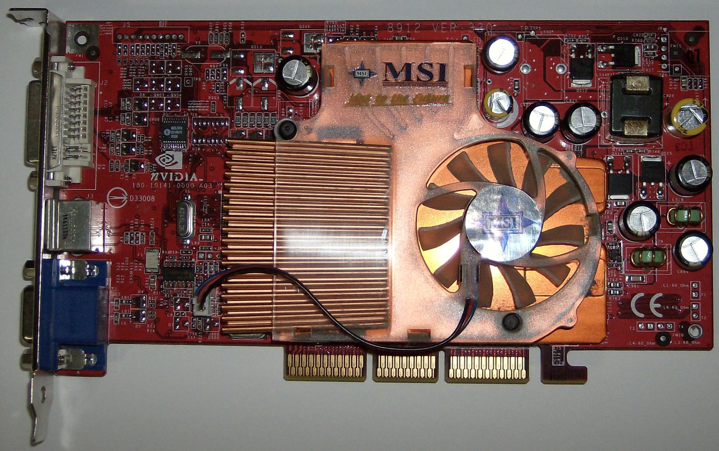
MSI FX5600XT-VTDR128 (MS8912) - 2003
The Geforce FX wasn't terribly good and we'll leave it like that. Part of this was that it had ATI's exceptional R300 to deal with: It was poor by comparison, but part of it was simply that the Geforce FX was underperforming on its own terms. The 5600 was refreshed once from the NV31 it appeared with to a "flip chip" NV36 and a corresponding bump in clock to 400 MHz. It was priced alongside the Radeon 9600 family, all of which beat the FX 5600 very soundly in everything except Doom3. At the time, two very big games were released, Doom3 and Half-Life 2. HL2 was optimised and coded for the Radeon 9700 (R300), Doom3 was a heavy OpenGL stencil and Z-buffer user, which Geforce FX was better at. Valve Software famously refused to use Geforce FX's 64 bit pixel shader modes and coded everything in 96 bit for the R300, which the Geforce FX series had to work in 128 bit for. A fan-made patch for Half-Life 2 rewrote many of the shaders to "hint" down to 64 bit when it wouldn't be noticed, hence gaining large amounts of performance on the Geforce FX without any video quality loss. With that patch, the FX 5600 was only slightly behind the Radeon 9600. But who pays the same money for less product? Core: NV31 with 4 ROPs, 1 TMU per ROP, 325 MHz (1,300 million texels per second) RAM: 128 bit DDR SDRAM, 550MHz, 8,800MB/s Shader: 2x PS2.0, 1x VS2.0 MADD GFLOPS: 8.5 Thanks to Ars AV forum member SubPar |
||||||||||||||||||
 |
ATI Radeon 9650 256 MB (Mac) - 2004
This rather bulky thing was common in PowerMac G5 machines way, way back. Apple loved to confuse people and hide the actual hardware which was on sale: The 9650 was significantly slower and more cheaply made than the 9600XT which was also available on G5 machines! You'd be spending six hundred US dollars for one of these. It clocked in at 400 MHz on the GPU, which controlled 270 MHz DDR memory at 128 bits wide. The GPU was fitted with a single R350-based quad (four pixel pipelines), two vertex shaders and four pixel shaders. It was capable of a shader throughput of about 12 MADD GFLOPS. The Radeon 9600 PRO ($120) was more or less the same, but with 300 MHz DDR memory, so it was in fact faster. The RV351 GPU was simply the RV350 with a Mac BIOS on its external BIOS chip - in terms of features and performance, it was identical to the RV350 in the Radeon 9600. For the Mac edition, a larger heatsink than usual was fitted (cooling in a G5 was horrendous) and it was given dual-DVI, while the S-video output was stripped off: Macs were intended to use highly profitable Apple displays or nothing. One of the DVI outputs was dual-link, able to run a 30", 2560x1600 Apple Cinema display, but the other was single link and limited to 1920x1080 or so. Adding insult to injury, ATI went and sold the EXACT SAME CARD as the "Radeon 9600 Pro Mac and PC edition", with dual-firmwares but without the actual Radeon 9600 Pro's 600 MHz memory clock. ATI released it at $199 USD, it was usually available around $170 or so. The previous PowerMac G4s commonly had fearsome Radeon 9700 GPUs, which were far more powerful than these, while the high end G5s had Radeon X800XTs, but Apple being Apple, the Mac edition of the X800XT ran its GPU at 473 MHz, the real version was rated at 500 MHz. It also cost - I shit you not - four and half times more. Mac video "solutions" were full of plain ol' PC video cards with slightly different BIOS firmware and down-rated. It was quite common for OS X suckers to go out, buy the PC version, and flash a Mac BIOS on it. For example, this Radeon 9650, bought from ATI by Apple and resold to you, would have been $599.95. The Radeon 9600 PRO (slightly faster) retailed around $120, the Radeon 9600 Pro Mac and PC edition - identical to this card, but officially and genuinely from ATI and guaranteed comaptible with the PowerMac G5 was $199 at launch. So you could give Apple $400 for... well... free money for Apple is always good, right? What about those wanting REAL POWER? (Caps!) ATI would sell you the workstation-class FireGL X1-256, a Radeon 9700 Pro with 256 MB on board and fiendishly powerful for $540. By 2004, the FireGL X3 was available, at a mite over $1,000, and the fastest workstation class video card in the world. Core: RV351 with 4 ROPs, 1 TMU per ROP, 400 MHz (1,600 million texels per second) RAM: 128 bit DDR SDRAM, 540 MHz, 8600 MB/s Shader: 4x PS2.0, 2x VS2.0 MADD GFLOPS: 12 Thanks to Ben |
||||||||||||||||||
|
TurboCache and HyperMemory About this time, both ATi and Nvidia produced GPU models with woefully insufficient video memory (VRAM). In an era where 128 MB was mainstream and the high end was sporting 256 MB, some of these cards had just 16 MB! The Geforce 6200 TC-16 used cheap DDR memory, a SINGLE chip of it on a 32 bit bus, running at 350 MT/s, for a bandwidth of just 5.6 GB/s. ATi used "HyperMemory" as exactly the same thing, extremely bottom of the barrel GPUs, based around the X300 part (RV370), with either 32 MB or 128 MB. ATi billed these as "128 MB HyperMemory" and "256 MB HyperMemory" respectively. This was an outright lie. Both ATi and Nvidia produced flashy diagrams showing how system memory could be quickly accessed over PCI Express so could be used just like VRAM. AGP had been doing this for years with the DiME feature, and PCIe 1.1 was not particularly faster than AGP 8X (4 GB/s and 2.1 GB/s, respectively) - It was well known that if AGP texturing had to be used, performance would stink. Had Nvidia and ATi found PCIe's magic secret sauce? No. Oh hell no. The TC/HM GPUs performed exactly as you'd expect a GPU critically low on VRAM to perform. ATi's own slides showed the X300 SE being almost beaten by an Intel i915 IGP in Half-Life 2. The same slides showed a 64 MB-equipped X300 SE spanking the hell out of a 16 MB GeForce 6200 TC-16. Hexus.net presented charts of the 32 MB versions of both GPUs delivering an utterly unlovable showing in all tested games. The X300 SE won, barely, due to its use of 64 bit RAM vs Nvidia's 32 bit. Neither of them gave any sort of good showing. Yet, Hexus managed to give it a "good value" award. Hattix.co.uk would argue a product which doesn't even work is not good value, regardless of how cheap. So... Why? Why would engineers, who clearly knew this was not going to work, push out deliberately knobbled products? There are five main expenses in video card manufacture, and usually in this order:
Additionally, there is usually just one capacity of DRAM which is the best value. In this era, it was the 256 Mbit (32 MB), 32-bit wide DDR DRAM rated to 333-366 MT/s. Two of those got you a 64 bit bus and 64 MB capacity. Putting 128 MB, which was really the necessary minimum, also necessitated the use of 512 Mbit DRAMs to match the 64 bit bus, which were twice the capacity but triple the price. You couldn't even come out ahead using a wider bus for the same capacity. A 128 Mbit DRAM was usually a yield harvested 256 Mbit, with half the DRAM turned off... and so only 16 bits wide, so you gained nothing. 32 bit 128 Mbit DRAMs were around 0.7x the price of the 256 bit, so one didn't save there either. The 256 MB GeForce 6800 models had a 256 bit bus and eight DDR DRAMs on each side of the PCB. For a <$50 video card, saving the $5 the extra DRAMs cost was a substantial saving. They could only handle much older games and, even then, at very poor performance levels. They were a cost-cutting curiousity, one which rightly failed. |
|||||||||||||||||||
|
Gainward GeForce 6600 128MB AGP - 2004 With an 8x1 pipeline clocked at 300MHz and 128 bit, 250MHz DDR, this had a pixel fill rate of 2400 megapixels per second and a memory bandwidth of 8000MB/sec. Looking closely at the core in the big image, it can be seen to be labelled "GF6800-A4", this quickly labelling it as the A4 revision of the NV40, most likely intended for a GF6800. Maybe it was a little faulty or maybe Nvidia just made too many of them, who knows. In whichever case, two of the 4x1 blocks were disabled to cut it down from 16x1 to 8x1 and it was plonked behind an AGP bridge chip (the little one at the bottom) to bridge the NV40's native PCIe to AGP. This bridged arrangement was collectively known as NV43 and used in the AGP versions of GeForce 6200, 6600 LE, 6600 and 6600 GT. It wasn't a great performer, the Radeon 9700 earlier on this page would quite easily beat it, but it did perform well with Shader Model 3.0 (which the 9700 didn't support) and was a good way of gaining SM3.0 support on an entry level to mainstream performance card but SM3.0 using games were just too intensive for the meagre 8GB/sec memory of the 6600. The fate of this card, after being kindly donated by Al Wall, was to have its AGP to PCIe bridge chip damaged during a heatsink replacement. It ended up at the bottom of a storage box until 2016, when it was finally discarded. Thanks to Al for his kind donation of the hardware Core: NV40 with 8 ROPs, 1 TMU per ROP, 300MHz (2400 million texels per second) RAM: 128 bit DDR SDRAM, 500MHz, 8000MB/s Shader: 8x PS3.0, 3x VS3.0 MADD GFLOPS: 28 |
||||||||||||||||||
|
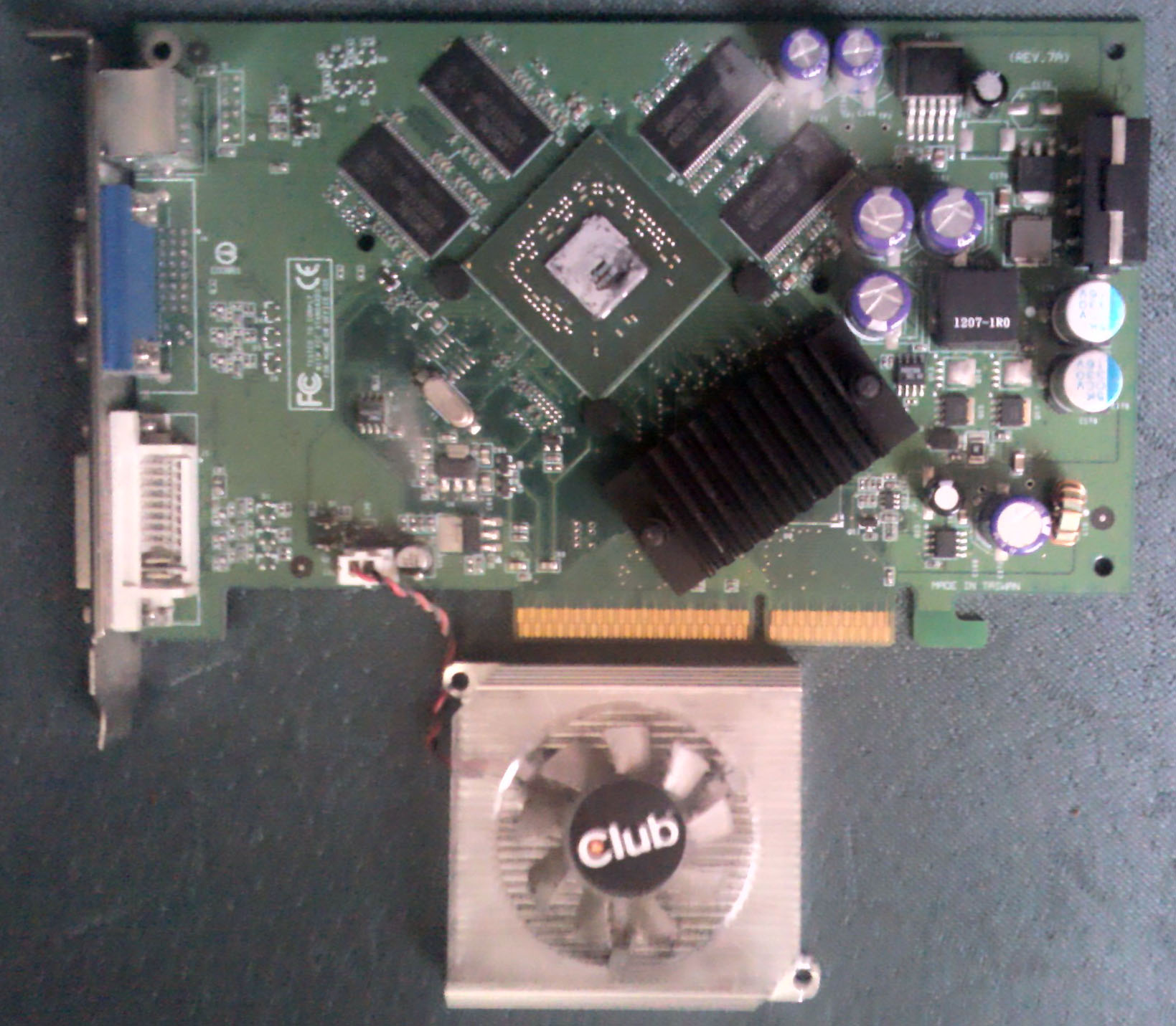
Club 3D GeForce 6600 256MB AGP - 2004 In general, this is nearly identical to the Gainward above, but the GPU is labelled "GF6600" and it has 256 MB onboard: Very likely, it is a later model from 2005 or so. When testing this, and seeing the "256 MB" on the pre-POST VGA BIOS splash, I had high hopes for the memory on this. Nvidia cards have always been a diverse lot, with plenty of completely non-standard cards from the different vendors, so the hope was that this'd have faster memory than normal. Instead it had slower memory! Club 3D had used standard DRAMs intended for PC3200 DIMMs. Cheap as all hell, but left the GPU starved. In the same system (a 3 GHz P4 Northwood with HT), the Radeon 9700 above could score 29,000 in Aquamark3, but this thing only managed 23,000. For what it's worth, the same Radeon 9700 coupled to an Athlon XP 3200+ was pushing well over 40,000. As an AthlonXP 3200+ and a Pentium4 3.0 are very similar, I suspected something was afoot. True enough, Throttle Watch told me that the P4 was throttling anything between 15% and 20% while running the tests. One heatsink-clean (eww) later, we had 25,200 out of the Geforce 6600 and 39,000 from the Radeon 9700. For comparison, the under-performing Radeon HD4250 IGP built into a cheap single-core AMD laptop (2.4 GHz) got 32,400. The GPUs themselves are of quite similar spec, in fact this GF6600 has a small advantage in terms of clock rate and shader model, as well as twice as much memory... But memory speed means much more than size. The R9700 could push over 17 GB/s, this thing just 6.4 GB/s. Core: NV40 with 8 ROPs, 1 TMU per ROP, 300MHz (2400 million texels per second) RAM: 128 bit DDR SDRAM, 400MHz, 6400MB/s Shader: 8x PS3.0, 3x VS3.0 MADD GFLOPS: 28 |
||||||||||||||||||
|
EVGA (?) GeForce 6800 GT 256MB PCI-E - 2004 Very roughly the same performance as the Radeon X800XT below, but also sold quite a bit worse than expected. Why? There were thirteen different models! In order of performance, they were 6800XT, 6800LE, 6800, 6800 GTO, 6800GS, 6800GT, 6800 Ultra, 6800 Ultra Extreme. Additionally, the 6800 GT, Ultra and Ultra Extreme had both AGP and PCI-E versions. The lowest end, the 6800XT, was actually slower than the fastest 6600, the GT, so nobody knew what the hell they were buying, sales were poor, so Nvidia introduced even more models. Nvidia introduced Shader Model 3.0 with the Geforce 6 series, which truthfully was just a minor extension to SM2.0 to relax instruction limits and introduce better flow control. The basic NV40 GPU was a 16 ROP, 16 pixel shader, 6 vertex shader device which was unfortunately dogged by enormous (for the time) power consumption and Nvidia had made such a complex GPU that it couldn't actually be manufactured very well (NV would repeat this with Fermi). The full NV40 GPU was only enabled in the 6800 GT, Ultra and Ultra Extreme and even then it was clocked quite low, no Geforce 6800 ever went faster than 450 MHz (the hilariously expensive Ultra Extreme) and most clustered between 350 and 400, while ATI's R420 was topping 500 MHz with ease. NV40 was over-ambitious and this made it expensive and power hungry. Additionally NV had still not caught up to ATI's phenomenally fast R300-based shaders, so the very fastest Geforce 6 still had about three quarters of the shader power of its Radeon competitor. NV40's derivation, G70 used in the Geforce 7 series, corrected these problems. Thanks to Kami Core: NV40 with 16 ROPs, 1 TMU per ROP, 350MHz (5,600 million texels per second) RAM: 256 bit GDDR3 SDRAM, 500MHz, 32,000MB/s Shader: 16x PS3.0, 6x VS3.0 MADD GFLOPS: 66 |
||||||||||||||||||
|
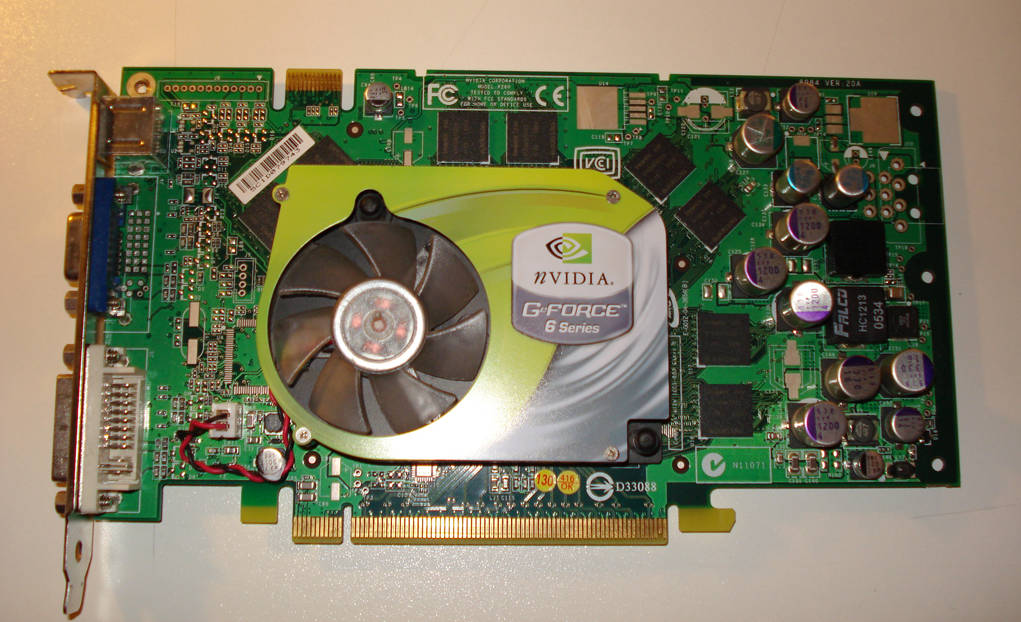
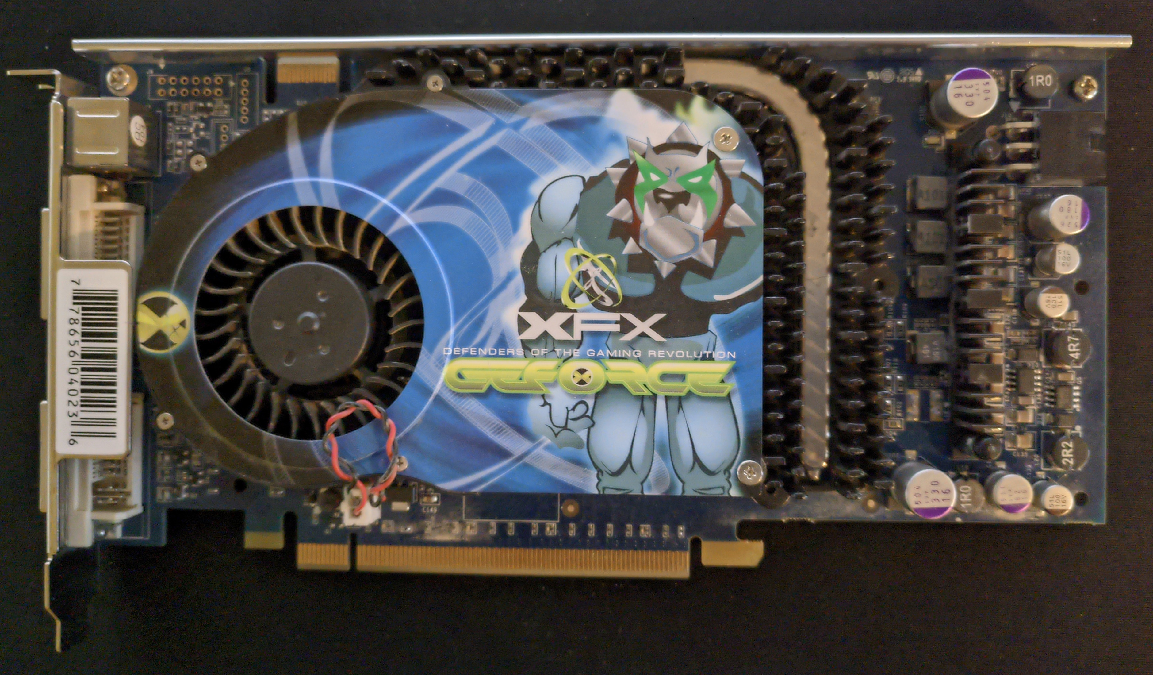
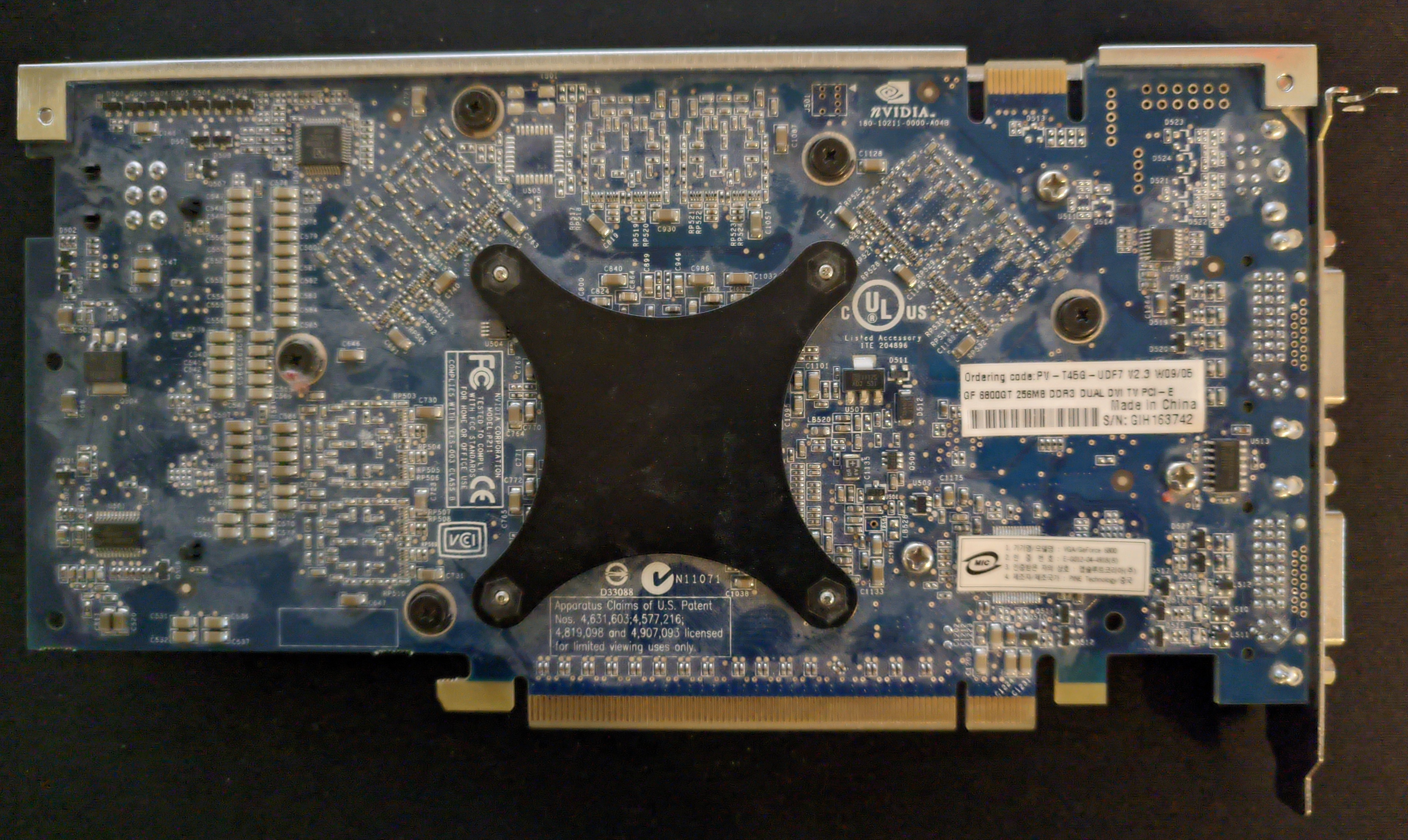
XFX GeForce 6800 GT 256 MB - 2004 What, then, the holy hell is this? An XFX Nvidia card?! In 2009, XFX switched from Nvidia to AMD. It did release a few Nvidia video cards afterwards, as far as some low end GT 640s, but that was it. Before then, XFX was purely an Nvidia partner and ATi/AMD was served largely by Club3D, MSI, and Sapphire. Nvidia was very aggressive with its board partners and would rarely tolerate anyone building products for the competition. XFX was the brand you went with when you wanted absolute rock solid peace of mind: It had a "double-lifetime" warranty. If you registered your purchase at XFX's website, you got a lifetime warranty and could transfer this to a subsequent buyer. So, technically, this GPU is still under warranty if its original owner had registered it. XFX discontinued this double-lifetime warranty in 2012, phasing it out for subsequent products after the Radeon Rx 200 series. XFX, like EVGA and the K|NGP|N branding, also linked up with competitive e-sports personality Johnathan "Fatal1ty" Wendel, for extremely high end over-engineered products. It is a corporate body of Hong Kong based Pine Group and operates out of California. This card was one of XFX's high end 6800GTs, there's an early version of what became XFX's "Alpha Dog" branding on it, even a cursory look tells you it's a quality engineered card. The card is one slot, not unusual for the day, and uses an axial blower with a single heatpipe. This same cooler design was also used by most other first generation 6800 GTs. While laughably small by today's standards, this was some very serious cooling performance for 2004. There's also a stiffening rod running down the card, as heavy coolers (how little they knew!) were concerning for some reviewers. Quality cards would have these stiffeners to prevent board sag, but it was not part of Nvidia's reference design. As it is only a single slot card, there's nowhere for the blower to exhaust but into the case, which is what it does: The blower appears to be "backwards" to the modern viewer. The board power is 75 watts, which 67 watts is allocated to the GPU. Nvidia's reference design is followed precisely, even down to the little silkscreened box above the PCIe slot which was meant to take a label. The PCIe version and AGP version had exactly the same PCB layout but for the edge connector, and the AGP version used a bridge chip mounted on the same substrate as the GPU. Additionally the AGP version used a four pin hard drive power connector instead of the PCIe six-pin. XFX's version appeared to not be factory overclocked (this was rare at the time, Albatron did a 365 MHz version) and would have run at the stock 350 MHz. RAM, 256 bit GDDR3, would run at 500 MHz (or 1,000 MT/s) for 32 GB/sec bandwidth. Most 6800 GTs would not go very far beyond 400 MHz. For those questioning why it is listed as "NV40" and not "NV45". NV45 refers only to the substrate, NV40 and HSI (PCIe to AGP bridge chip) used in the AGP version. Thanks to deathterrapin Core: NV40 with 16 ROPs, 1 TMU per ROP, 350MHz (5,600 million texels per second) RAM: 256 bit GDDR3 SDRAM, 500MHz, 32,000MB/s Shader: 16x PS3.0, 6x VS3.0 MADD GFLOPS: 66 |
||||||||||||||||||
|
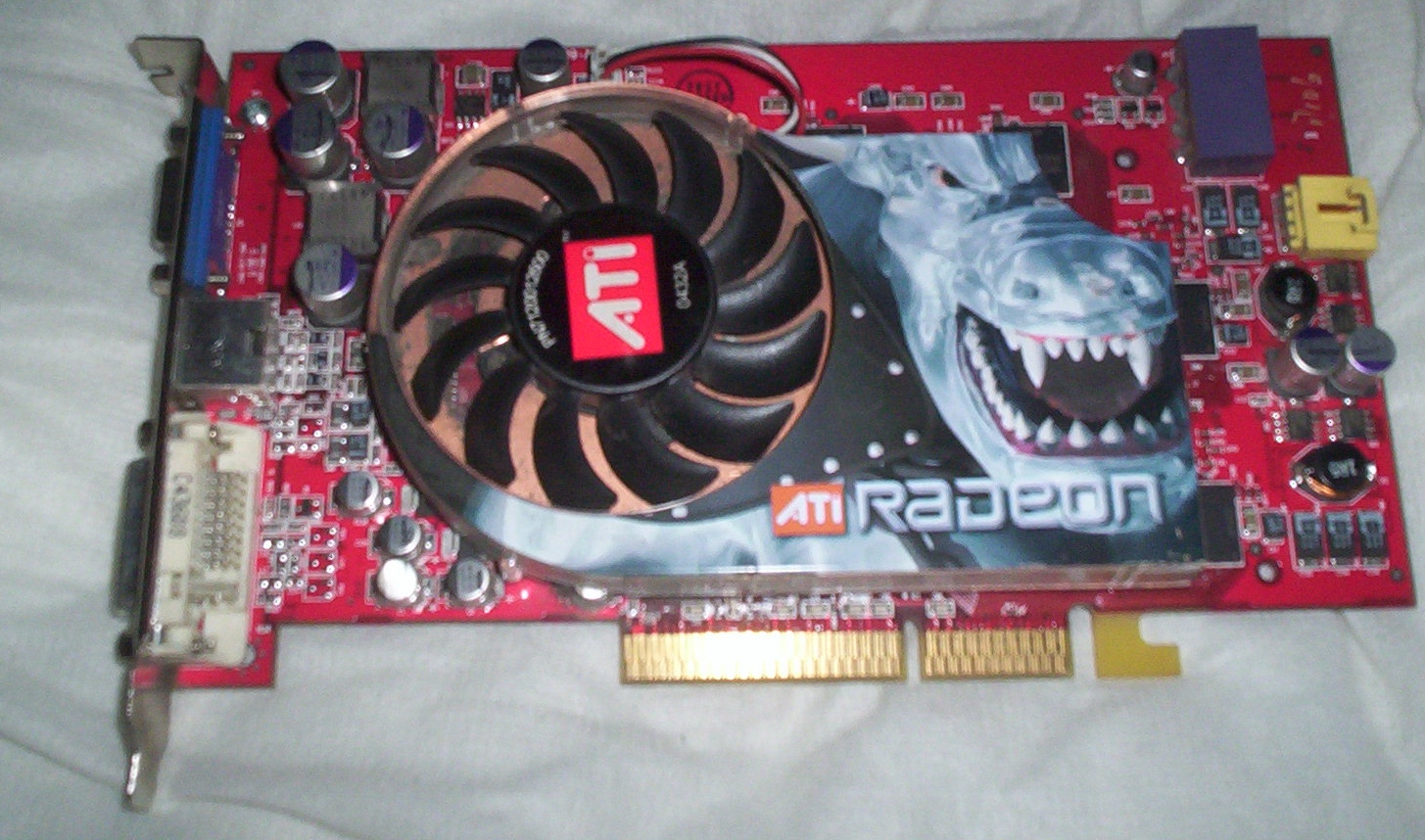
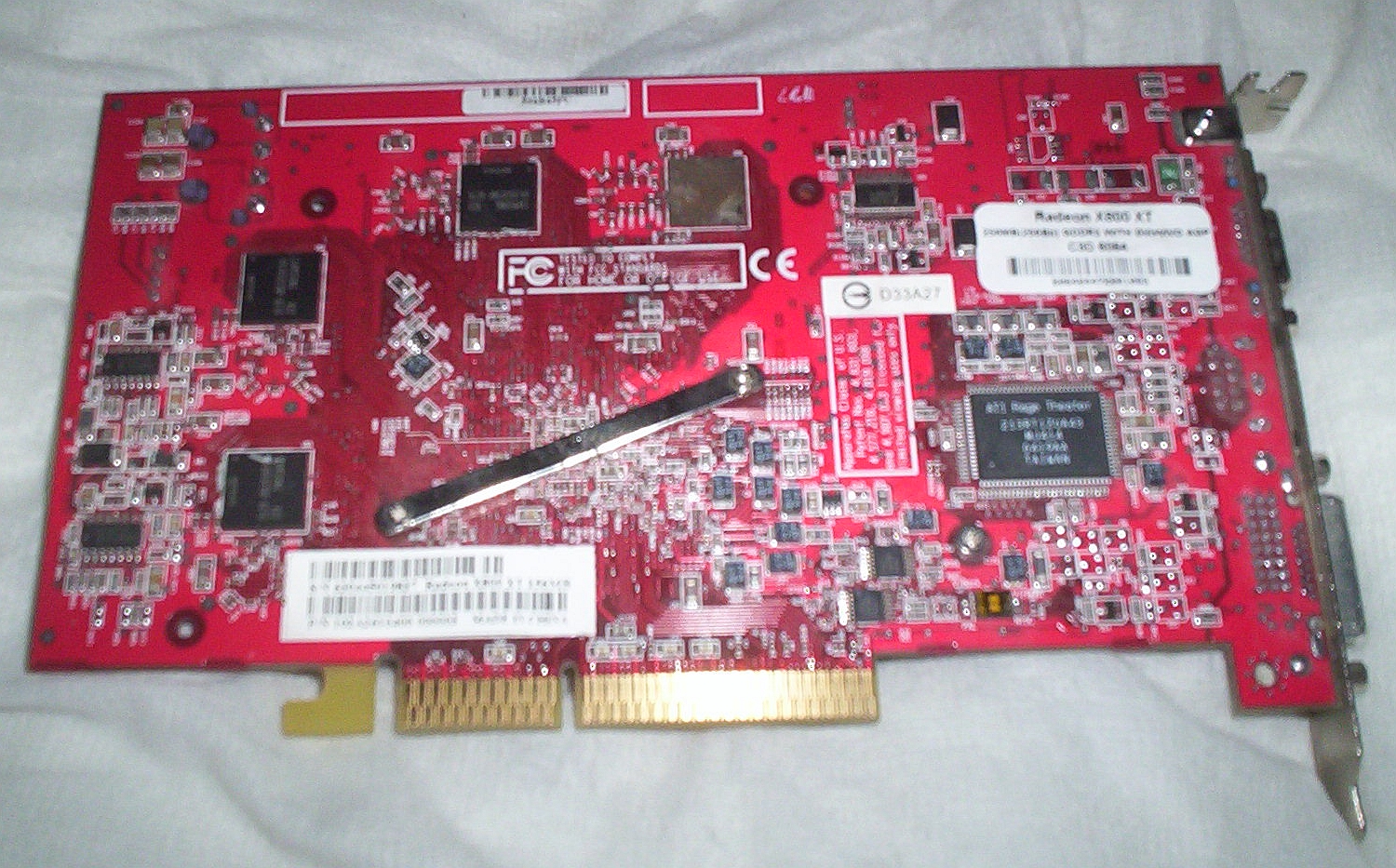
Radeon X800XT 256MB VIVO AGP - 2004 The R420 GPU was a stop-gap solution never really intended for release. The actual R420 was to become the R6xx series (Radeon HD2xxx) and was plagued by delays and problems from day one, problems that even when it was finally released it was barely working at all. R420 as released was R390, basically two R360s in tandem on the same die and a sort of contingency plan. When NV40 was much, much faster than ATI had expected, R390 had to be expedited to release, yesterday. It took the R420 codename and was quickly adapted to a 130nm TSMC process. However, its age showed. At heart it is a direct descendant of R300 (see above) and it shares many of the same shader limitations. It did relax some limits, it wasn't full Shader Model 3.0, it was "2.0b". Shader Model 3.0 was really hyped up by Nvidia but, to developers, it was more a "2.1" version, didn't really add all that much. In general anything possible on SM3.0 was also possible on SM2.0b of the Radeon X series. The GPU design also showed its R300 heritage: Vertex shaders were decoupled from the core (so every R4xx product had six vertex shaders) but pixel shaders were not. Each quad (four ROPs) had four pixel shaders and so this 16x1 ROP design had 16 pixel shaders. This was the exact same design first introduced in the Radeon 9700, which had four 'global' vertex shaders and four pixel shaders per quad. The X800XT and Geforce 6800 Ultra traded places at the top of benchmarks throughout their production life, neither one having a decisive advantage. NV40 was a more efficient, more elegant part, but it was also limited to a top speed of 400 MHz and had a sizeable shader performance disadvantage. In terms of raw pixel shader power, R420 was a little less efficient than NV40 (because NV40 could use SM3.0 shaders) but clock for clock about 30% more powerful. When running SM2.0 shaders, NV40's efficiency savings evaporated and the raw performance advantage of R420 (which was also clocked higher) came into play. Core: R420 with 16 ROPs, 1 TMU per ROP, 500MHz (8000 million texels per second) RAM: 256 bit GDDR3 SDRAM, 500MHz, 32000MB/s Shader: 16x PS2.0b, 6x VS2.0 MADD GFLOPS: 94 |
||||||||||||||||||
|
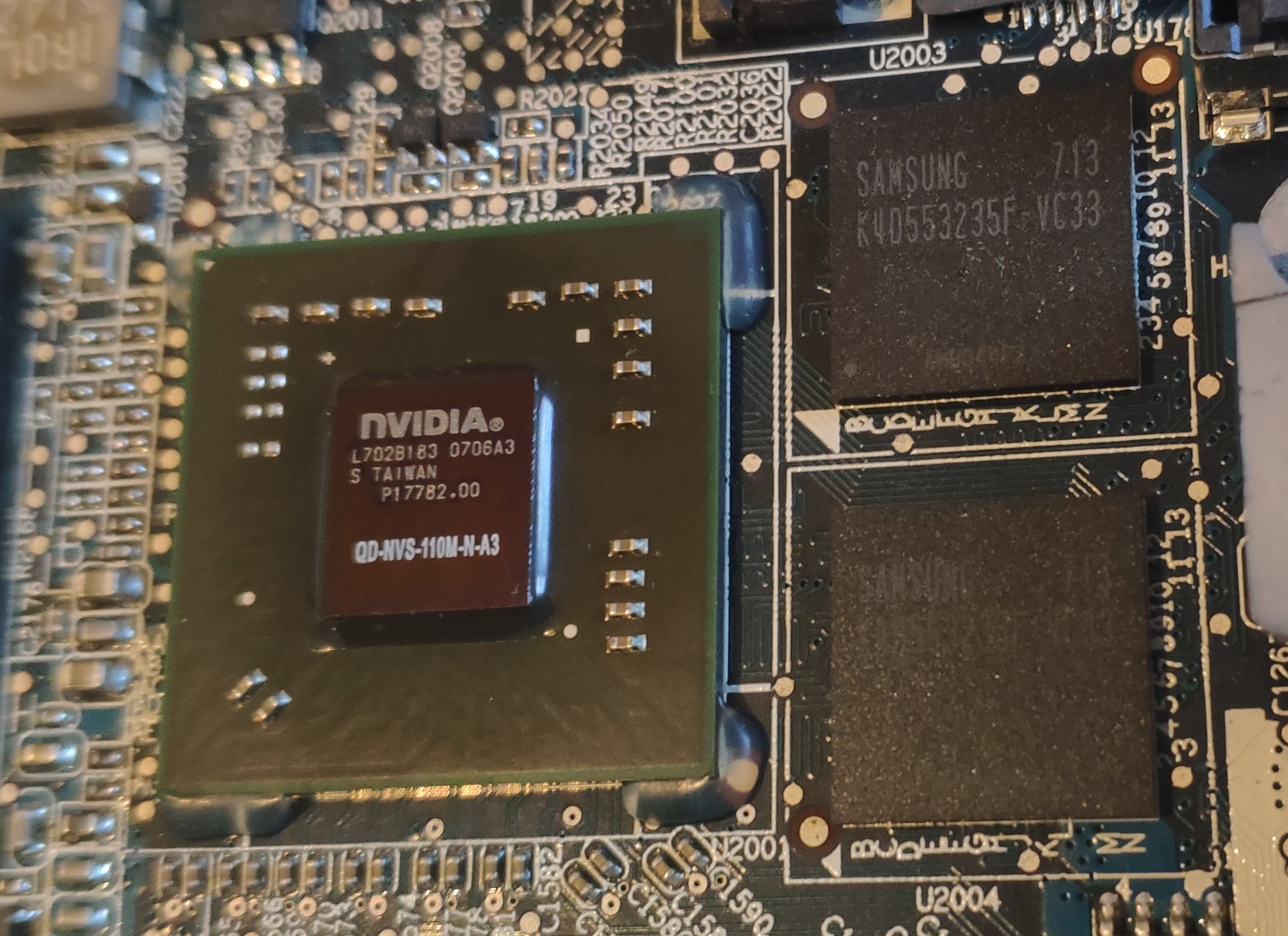
Nvidia Quadro NVS 110M 256MB - 2006 This isn't a video card. It's got most of the components of one, two RAM chips and a tiny GPU. The GPU has a production marking, the laser-engraved NVIDIA logo and the production code (with the date code of 0706) and then a binning marking telling us which product it was destined for at the binning stage. Sometimes the binned product is higher than the sold one, but never lower. Quadro NVS 110M was the lowest performing member of the GeForce 7 family. In fact, some of the more decent IGPs could out perform it, such as AMD's Radeon HD 4250 with sideport memory. Quadro NVS 110M was optimised for very low power, so it only ran at 300 MHz. The RAM, likewise, clocked at just 300 MHz. In all, it had a TDP of 10 watts, lower than the chipset in the same laptop - Which was a Dell Latitude D620. The spec for the Quadro NVS 110M was 512 MB RAM, but this used only 256 MB, still twice as much as a GPU of this level really required. Core: G72 with 2 ROPs, 4 TMU , 300MHz (1,200 million texels per second) RAM: 64 bit DDR SDRAM, 300MHz, 4800MB/s Shader: 4x PS3.0, 3x VS3.0 MADD GFLOPS: 8 |
||||||||||||||||||
|
eVGA Geforce 7900 GTO 512MB - 2006 The 7900 GTO was something of a surprise when it was released in June 2006, it had not been announced, no PR was sent and suddenly vendors had the outrageously cheap 7900 GTO in stock. It is, for all intents and purposes, an underclocked 7900 GTX made for OEM customers. It had the 7900GT's memory bandwidth and the 7900GTX's GPU speed. The GTX has 800MHz GDDR3 memory, the GTO has merely 660MHz GDDR3 memory, giving the GTO 41.3GB/s memory bandwidth to its 512MB of onboard RAM. Both have a 650MHz GPU, 24 ROPs, 24 pixel shaders, 8 vertex shaders and Shader Model 3.0 support. Apparently, some Geforce 7900 GTX cards had faulty RAM so rather than absorb the losses, Nvidia recalled them, flashed the BIOS to underclock the RAM, and patched the hardware ID from "0290" (7900 GTX) which was in the hardware to the "0291" that the much slower Geforce 7900 GT used. Under a sticker on the back of this eVGA card is the designation "Geforce 7900 GTX 512MB" but the sticker says "Geforce 7900 GTO 512MB". The RAM problem remained, however, and while the GTX used the very same RAM chips (most GTOs would overclock that far), this one will not pass 1460 MHz memory, the GTX was clocked at 1600 MHz. The G70/G71 GPU is the 'full version' of the GPU in the Playstation3 and a development of NV40, the Geforce6 series base GPU. The cooler on this card has been replaced by a Zalman CNPS "Flower" which, rather annoyingly, doesn't have the correct fan fitting for the video card so can't be automatically controlled by the video card. The card was a monster to put it simply. It performed within a hair of the much more expensive 7900 GTX and beat the 7950 GT by that same hair. This card eventually died in August 2011 when the third party heatsink's fan connector failed, leaving the GPU without cooling for several days, by which time it had suffered fatal damage. Update: In April 2012, it was resurrected. Turns out a capacitor (the right-most on the image) had been knocked off the PCB. Replacing it with a large electrolytic from the box 'o spares means it works normally. Some boots don't detect it, but this may well be an artefact of the rather cruelly bodged up system it's in (including the Opteron 165 from the CPU section!). Update 2!: In 2015 it was donated to Ben (the same guy behind the PowerMac G5's GPU) after sitting on a shelf for a while, and turned out to not work anymore. It ended up in Ben's bin. Core: G71 with 16 ROPs, 24 TMUs, 660MHz (15.7 billion texels per second, 10.4 billion pixels per second) RAM: 256 bit GDDR3 SDRAM, 1320MHz, 42240MB/s Shader: 24x PS3.0, 8x VS3.0, MADD GFLOPS: 301 The 300+ GFLOPS of the G71 was originally thought to be a typo, G70 could only peak at perhaps 180 GFLOPS, G71 optimises commonly used loop and branch functions to stop them stalling the execution units, so doesn't actually have more hardware available but it can use what it has much better than G70. In shader heavy benchmarks, G71 will wipe the floor with G70 even at the same clock. |
||||||||||||||||||
| Just what is a pixel shader anyway? |
Nvidia and ATI had been, for a long time, adding slightly programmable portions to their GPUs. NV15 (Geforce 2) had a bank of register combiners, which is part of an ALU, the part of a CPU that "does the work". It used this for its triangle setup and T&L engine, drivers were able to customise how it worked for different games and so gain maximum performance. These devices were called "shaders" in engineering parlance, since their most common use was to solve lighting equations per-pixel. Their origin can be traced as far back as the Voodoo3's guardband culler, a piece of hardware which assisted in rotating triangles in 3D space to be correctly oriented with respect to the view frustrum. TNT2 and Rage 128 also had similar hardware. The origin in the lighting and transformation engine gave us two types of shader. One was dedicated to operating on RGB data, textures, pixels, colours; This was the pixel shader and came from the device used to solve lighting equations. The other was higher precision but slower and more complex, it was used to alter vertex positions, it came from the transformation and setup part of the engine. Microsoft saw what was going on (as they control DirectX, they have a very big say in what GPUs can and cannot do) and decided that a standardised model for what a shader should be able to do was needed. DirectX 8.0 included shader model 1.0 which was based around the capabilities of the shaders in the Geforce 3, since it was also the DirectX model used in the X Box, which also had GeForce 3 level video. An earlier version, shader model 0.5, was based around what a Geforce 2 could do but was deemed too inflexible to expose to programmers in the Direct X API. It can be addressed with some NV specific OpenGL extensions, but few used them. Nvidia launched GeForce 3 with great fanfare in 2001, claiming this was a brand new world of cinematic gaming effects with the Nvidia "Kelvin" architecture and "fully programmable pixel shader hardware". In truth, Shader Model 1.1 was extremely inflexible, had a very tight instruction limit, and was used only to provide basic "bloom" effects. Usually, very badly. GeForce 3 was very expensive, didn't perform any better than the previous generation and, by the time games were using DirectX 8 shader effects, GeForce 3 was too slow to offer decent performance in them. While Nvidia wants us all to believe GeForce 3 was the first pixel-shader equipped GPU, shader model 2.0 was really the birthplace of the modern GPU and its harbinger was the ATI R300 (in the Radeon 9700). Nvidia also had a very flexible shading part, NV30 (Geforce FX 5800) which was in many ways far more powerful than the R300 (while slower in raw crunch rate, it could do more in fewer instructions and had fewer restrictions). The two were, however, solving the same problem in different ways. Microsoft did not want to split the shader model in half, Direct X was only ever going to support one shader model and it was ATI's. SM2.0 was based around what the R300 could do so NV30 was left having to emulate capabilities it didn't have. R300 was fixed at 24 bit precision in SM2.0, but NV30 had 12, 16 and 32 bit modes - no 24 bit. NV30 had to emulate 24 bit using its 32 bit mode which was just less than half as fast as the 16 bit mode and often gave no advantage. Shader Model 3.0 was designed around what NV40 could do, putting ATI at a considerable disadvantage, their extended SM2.0 (SM2_b, seen in R360 and above, which is R9600, R9800 and the Radeon Xx00 family, such as the Radeon X800 XT I used to have) was similar to Nvidia's SM3.0, and most developers will tell you SM3.0 was really more of a "2.1" version. Finally, Shader Model 4.0 with DirectX 10 unified the shaders, which had become as complex as simple CPUs anyway, doing away with vertex shaders and pixel shaders to provide a single unified shader. This was good, very good. Most games used a 80:20 split between pixel and vertex shaders, but occasionally they'd reverse it, which caused momentary losses of framerate. This meant that hardware was made for the most common case: The G71 in the Geforce 7900 series (see below) had 24 pixel shaders and 8 vertex shaders with a pixel shader performance of about 250 GFLOPS (billion floating point operations per second) but it had significantly poorer vertex performance, everything did, because vertex operations are so much more complex than simple RGB pixel operations and it had fewer units, games only used 20% of their shading time doing vertices. |
||||||||||||||||||
 Hattix hardware images are licensed under a Creative Commons Attribution 2.0 UK: England & Wales License except where otherwise stated.